


Introduction
Ceramic substrates are used in electronic and power applications where electrical insulation, thermal management, dimensional stability and reliability need to be considered together.
Selecting a ceramic substrate is not simply a matter of choosing the material with the highest thermal conductivity. The ceramic material, substrate structure, metallization or copper joining technology, geometry, thermal expansion behavior and operating conditions all influence the final performance of the assembly.
This Technology Hub brings these engineering considerations together to help engineers understand ceramic substrate technologies, compare material options, evaluate design factors and identify common failure mechanisms.
Ceramic Substrate Engineering Fundamentals
A ceramic substrate provides an electrically insulating and thermally conductive foundation for electronic assemblies.
In a typical power electronic assembly, heat generated by a semiconductor device must pass through several interfaces before reaching the cooling system:
Semiconductor Device → Attach Layer → Copper Layer → Ceramic → Baseplate → Heat Sink
The ceramic layer therefore plays more than one role. It must provide electrical isolation while also supporting the required thermal path and maintaining structural integrity during temperature changes and mechanical loading.
The appropriate substrate depends on the complete system rather than on a single material property.
How to Select Ceramic Substrate Materials
Different ceramic materials provide different combinations of thermal, mechanical, electrical and processing characteristics.
Material selection should begin with the requirements of the application rather than with a simple ranking of materials.
Alumina (Al₂O₃)
Alumina is widely used where electrical insulation, established processing routes and cost considerations need to be balanced. Consider alumina when:
- General electrical insulation is required
- Moderate thermal management is acceptable
- Manufacturing maturity and cost are important
- The application does not require the highest thermal conductivity
Typical considerations: cost, insulation, processing maturity and dimensional requirements.
Aluminum Nitride (AlN)
Aluminum nitride is considered when higher thermal conductivity is required while maintaining electrical insulation. Consider AlN when:
- Heat dissipation is a major design requirement
- Power density is relatively high
- Electrical insulation must be maintained
- Thermal expansion behavior is important to the package design
Typical considerations: thermal performance, material quality, processing and cost.
Silicon Nitride (Si₃N₄)
Silicon nitride is often considered for applications where mechanical strength and resistance to thermal cycling are important alongside thermal management. Consider silicon nitride when:
- Mechanical reliability is a major concern
- Thermal cycling is demanding
- The substrate is exposed to significant thermomechanical stress
- Long-term structural reliability is important
Typical considerations: strength, fracture resistance, thermal cycling and joint reliability.
ZTA and Other Ceramic Options
Zirconia-toughened alumina (ZTA) and other engineering ceramics may be considered for applications where mechanical performance, toughness or specific processing requirements influence material selection.
The appropriate material depends on the actual substrate function, geometry, operating environment and joining requirements.
Ceramic Substrate Technology
Ceramic substrates can be used in different structural and metallization configurations depending on the function of the final assembly.
At a high level, the technology path can be understood as:
Ceramic Material → Ceramic Substrate → Surface Metallization / Copper Joining → Circuit or Interconnection Structure → Final Assembly
Common technologies encountered in ceramic substrate engineering include:

The ceramic serves primarily as an insulating and structural material and may undergo grinding, polishing, laser processing or other precision operations according to the application.

A conductive or brazable metallization layer is formed on selected ceramic surfaces. The metallized surface can then support subsequent joining or electrical connection processes.

DBC technology uses a high-temperature bonding process to join copper to a suitable ceramic surface. It is widely associated with ceramic substrates used in power electronic assemblies.

AMB uses an active brazing system to join metal to ceramic. The technology is particularly relevant when the ceramic, metal system and reliability requirements call for an active brazing approach.
Ceramic Substrate Design Considerations
Material selection is only one part of ceramic substrate design. The substrate must also be evaluated as part of the complete thermal, electrical and mechanical system.
-
Thermal Conductivity
Thermal conductivity affects the ability of the ceramic layer to transfer heat away from the semiconductor device.
However, the overall thermal path also depends on:
- Ceramic thickness
- Copper layer
- Attach layer
- Baseplate
- Thermal interface materials
- Heat sink design
Therefore, ceramic thermal conductivity should be evaluated as part of the complete thermal path.
-
Coefficient of Thermal Expansion
Differences in coefficient of thermal expansion (CTE) between ceramics, metals, semiconductors and joining materials can generate thermomechanical stress during temperature changes.
CTE should therefore be considered together with:
- Material combination
- Joint structure
- Component geometry
- Temperature range
- Thermal cycling conditions
-
Ceramic Thickness
Ceramic thickness influences thermal resistance, mechanical behavior and dimensional stability.
The appropriate thickness depends on the material, substrate dimensions, thermal requirements, mechanical loading and manufacturing process.
-
Copper or Metallization Structure
For metallized and copper-bonded substrates, the conductive layer is part of the mechanical system as well as the electrical system.
Copper thickness, pattern geometry, coverage and distribution can affect thermal behavior, stress distribution and warpage.
-
Flatness and Warpage
Flatness and warpage can influence assembly quality, contact conditions and downstream joining processes.
Warpage should therefore be considered during:
- Material selection
- Substrate design
- Copper pattern design
- Joining process
- Thermal processing
-
Geometry and Machining Features
Holes, slots, steps, edges and other geometric features can influence stress concentration, machining behavior and final dimensional stability.
Complex structures should be evaluated together with the ceramic material and manufacturing process.
Common Ceramic Substrate Failure Modes
Ceramic substrate reliability depends on the interaction between material properties, substrate geometry, joining processes and operating conditions.
Common failure mechanisms include:
| Failure Mode | Engineering Factors to Evaluate |
|---|---|
| Ceramic Cracking | Thermal stress, mechanical loading, geometry, thermal cycling |
| Copper Delamination | Interface quality, joining process, thermal cycling |
| Solder Fatigue | Repeated thermal cycling, joint structure, CTE differences |
| Warpage | Material/process mismatch, copper distribution, thermal stress |
| Edge Chipping | Machining, handling, edge geometry |
| Interface Defects | Surface condition, joining parameters, metallization quality |
Failure analysis should focus on the complete assembly rather than treating the ceramic material as an isolated component.
Ceramic Substrate Engineering Selection Guide
A practical ceramic substrate selection process can be organized into six steps.
The best ceramic substrate is not necessarily the material with the highest individual performance. It is the solution that provides an appropriate balance between material properties, design requirements, manufacturing feasibility and system reliability.
-
1 — Define the Application Conditions
Identify:
- Power and heat generation
- Operating temperature
- Thermal cycling
- Electrical insulation requirements
- Mechanical loading
- Environmental conditions
-
2 — Select the Ceramic Material
Compare candidate materials based on:
- Thermal performance
- Mechanical properties
- CTE
- Electrical characteristics
- Processing requirements
- Cost considerations
-
3 — Select the Substrate Technology
Determine whether the application requires:
- Bare ceramic
- Metallized ceramic
- DBC
- AMB
- Other circuit or joining structures
-
4 — Define the Substrate Geometry
Review:
- Length and width
- Ceramic thickness
- Flatness / warpage
- Holes and slots
- Steps and recesses
- Edge geometry
- Dimensional tolerances
-
5 — Define the Metal and Interconnection Requirements
For metallized or copper-based structures, define:
- Metal system
- Copper thickness
- Pattern geometry
- Surface finish
- Joining method
- Electrical requirements
-
6 — Evaluate Reliability
Finally, consider:
- Thermal cycling
- Thermomechanical stress
- Interface reliability
- Warpage
- Ceramic cracking risk
- Assembly conditions
Ceramic Substrate Manufacturing Considerations
The manufacturing process can influence the dimensional stability, surface condition and reliability of a ceramic substrate. Manufacturing decisions should be made together with the material and design requirements rather than treated as a separate final step.
Typical manufacturing considerations include:

Material preparation and forming establish the basic geometry and density distribution of the green body.

Sintering converts the formed ceramic body into a dense ceramic structure. Shrinkage and process control can influence final dimensions and flatness.

Grinding, lapping, polishing and other machining processes may be used to achieve the required dimensions, surface condition and geometric features.

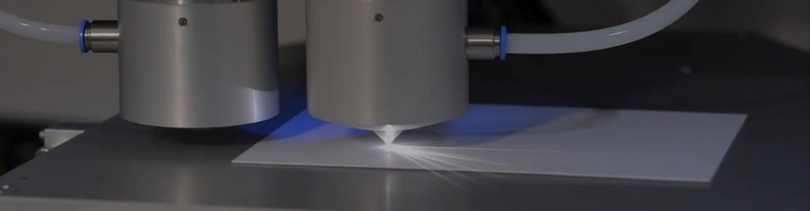
Laser processing can be considered for cutting, scribing, grooving or producing selected geometric features, depending on the ceramic material and design.

Selected ceramic surfaces may be metallized or joined with conductive materials according to the intended electrical or assembly function.

Typical inspection considerations include:
- Dimensional accuracy
- Flatness and warpage
- Surface condition
- Geometric features
- Metallization or interface condition where applicable
Ceramic Substrate Engineering Articles
Explore focused technical articles covering ceramic substrate materials, design, reliability and manufacturing.
Browse all metallized ceramics articles →
- Fundamentals & Design
- Material & Thermal Management
- Manufacturing & Metallization
- Failure Analysis & Applications
What Is a Ceramic Substrate?
Understand the basic structure, functions and application considerations of ceramic substrates.
Browse Article →
EV Power Modules Are Increasingly Using Silicon Nitride Substrates
electric vehicle (EV) power modules are facing higher thermal loads, more stringent thermal cycling, and higher reliability requirements.
Browse Article →
Alumina vs AlN vs Si₃N₄
Compare three commonly considered ceramic materials from the perspectives of thermal performance, mechanical behavior, CTE, reliability and application requirements.
Browse Article →
Thermal Conductivity in Ceramic Substrates
Understand how ceramic thermal conductivity interacts with substrate thickness, interfaces and the overall thermal path.
Browse Article →
Power Module Ceramic Substrates Guide
Explore the role of ceramic substrates in power module design and the relationship between thermal management, material selection and reliability.
Browse Article →
Ceramic Substrate Manufacturing Process
Follow the major manufacturing stages from ceramic forming and sintering to precision processing and inspection.
Browse Article →
Laser Cutting of Ceramic Substrates
Understand the role of laser processing in substrate cutting, scribing and selected geometric features.
Browse Article →
Ceramic Substrate Warpage
Understand the causes of ceramic substrate warpage and the factors that should be considered from design through manufacturing.
Browse Article →
Why Do DBC Substrates Delaminate
Review delamination:root causes, failure analysis and prevention guide
Browse Article →
Ceramic Substrates for Automotive Sensors
This guide explains how ceramic substrates are used in automotive sensors, compares common ceramic materials, discusses design considerations, and highlights manufacturing technologies that improve long-term reliability.
Browse Article →
Ceramic Substrate Applications
Ceramic substrates are considered in applications where thermal management, electrical insulation and reliability need to be evaluated together.
Power Semiconductor Modules
Ceramic substrates can provide electrical insulation and a thermal path within power semiconductor assemblies.
SiC Power Electronics
As switching devices operate at higher power density and temperature, substrate material and thermomechanical design become important considerations.
Electric Vehicle Power Electronics
Ceramic substrates may be used in inverter and other power electronic assemblies where thermal cycling and reliability are important design factors.
Renewable Energy Systems
Power conversion equipment for solar and other renewable energy systems may use ceramic substrates where thermal management and electrical insulation are required.
Industrial Power Electronics
Industrial drives, converters and other power electronic equipment may use ceramic substrates where thermal, electrical and environmental requirements exceed the capabilities of conventional substrate materials.
Need Help With a Ceramic Substrate Design?
Choosing a ceramic substrate involves more than selecting a ceramic material.
If you have a drawing, material requirement, substrate dimensions, thermal conditions or application information, our engineering team can review the requirements and help determine a suitable manufacturing route.
Share your drawing or project requirements with us.
Material selection should consider thermal performance, electrical insulation, mechanical requirements, CTE, thermal cycling, geometry, manufacturing process and cost. No single ceramic material is optimal for every application.
Ceramic thickness can influence thermal resistance, mechanical behavior, dimensional stability and manufacturability. The appropriate thickness depends on material, substrate size, thermal requirements and mechanical conditions.
Cracking may be associated with thermomechanical stress, thermal cycling, mechanical loading, geometric stress concentration, material combinations or manufacturing and handling conditions. Failure analysis should consider the complete assembly.
Copper delamination can be related to interface quality, joining conditions, thermal cycling, material combinations and stress distribution. The specific mechanism should be evaluated based on the substrate technology and assembly structure.
DBC and AMB should be evaluated according to the ceramic material, copper requirements, substrate geometry, thermal cycling conditions, joining requirements and overall assembly process. The appropriate technology is application-specific.
Excessive warpage can affect contact conditions, alignment, attachment quality and subsequent assembly processes. Warpage should therefore be considered during substrate design, material selection, metal-layer design and manufacturing.
Alumina is often considered when cost and established processing are important. AlN is considered when higher thermal conductivity is a major requirement. Silicon nitride is considered when mechanical strength and thermal cycling reliability are particularly important.
The final choice should be based on the complete application requirements.