

Introduction
Bare ceramic substrates are the ceramic base layers used in DBC (Direct Bonded Copper) and AMB (Active Metal Brazing) substrates. The ceramic substrate manufacturing process is just as important as material selection. Engineers and purchasing professionals often focus on choosing between Al₂O₃, AlN, and Si₃N₄, but may overlook an important fact: even when the same material is used, substrates produced by different manufacturers can vary significantly in thermal conductivity, flatness, and long-term reliability.
We often hear customers ask us: “Isn’t ceramic substrate manufacturing basically just pressing and sintering?”
The reality is far more complicated. What truly sets products apart is often not the material itself, but how well each manufacturing process is controlled.
In this article, we share our practical experience in manufacturing bare ceramic substrates made from Al₂O₃, AlN, and Si₃N₄. If you are still deciding which material is right for your application, see our guide to Al₂O₃ vs. AlN vs. Si₃N₄ for power modules. We break down the complete manufacturing process, from powder preparation to finished-product shipment, and focus on what needs to be controlled at each stage, why it matters, and what problems can occur when process control is inadequate.
Overview of the Bare Ceramic Substrate Manufacturing Process
The overall process typically includes ceramic powder preparation, forming, debinding and sintering, flattening, laser cutting, lapping and polishing, inspection, and packaging.
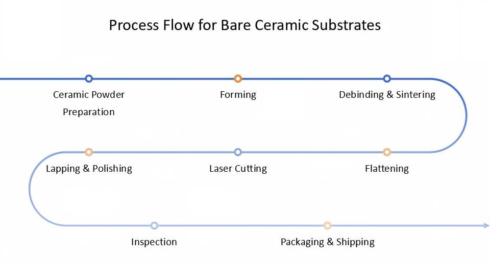
These eight steps are closely interconnected. A deviation in one process can carry over to the next and ultimately affect the yield and reliability of the substrate.
Let’s take a closer look at each step.
Ceramic Powder Preparation
Ceramic powder provides the foundation for the final performance of the substrate. Even when the same production equipment and process parameters are used, low-quality powder can still result in excessive porosity, unstable shrinkage, or inadequate thermal conductivity after sintering.
Al₂O₃ Powder
Al₂O₃ powder technology is relatively mature, with a stable supply chain. Standard insulating substrates commonly use 96% alumina.
For applications requiring higher thermal conductivity or electrical insulation performance, powders with a purity of 99% or higher may be selected.
Our actual test results show that 99% alumina typically has approximately 5%–8% higher thermal conductivity than 96% alumina. However, final performance still depends on the quality of the powder itself, sintered density, and the specific manufacturing process.
AlN Powder
AlN substrate performance is highly sensitive to powder quality, with oxygen content being one of the most critical parameters. Higher oxygen content can reduce the thermal conductivity of the sintered AlN.
For powders used in our high-thermal-conductivity AlN substrates, we normally control the oxygen content below 1.0%. Each incoming batch is tested, and any batch that fails our requirements is rejected.
Si₃N₄ Powder
Sintering additives must be added when preparing the Si₃N₄ matrix. At the same time, the ratio of α-phase to β-phase transformation needs to be controlled.
The α-phase content affects phase transformation and densification during sintering, so it needs to be controlled together with the sintering-aid formulation and sintering schedule.
Forming: Tape Casting vs. Dry Pressing
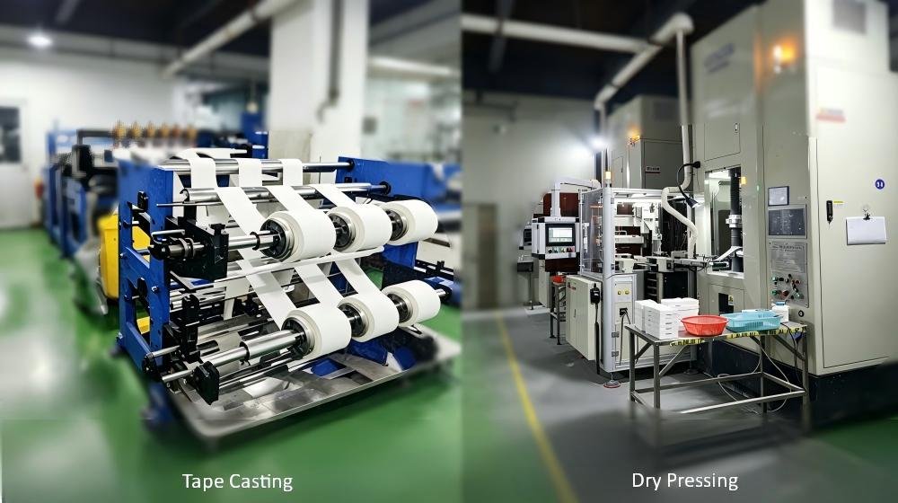
The choice of forming method depends on the application:
Tape Casting
Tape casting is the mainstream forming process for power module substrates. In this process, ceramic powder is mixed with solvents, dispersants, and binders to form a slurry. The slurry is then cast into a thin sheet using a doctor blade and dried to obtain a green body.
Under suitable material and process conditions, tape casting can produce green sheets as thin as approximately 0.1 mm, with thickness tolerances controlled within ±0.05 mm. It can also consistently produce thin specifications such as 0.25–0.635 mm while maintaining precise thickness uniformity across the entire sheet.
For these reasons, tape casting is widely used for ceramic substrates in power module applications.
Dry Pressing
Dry pressing is suitable for thick-film substrates and structural components. In this process, ceramic powder is directly filled into a mold and pressed into shape.
Although tooling costs are relatively high, the production cost per piece is lower. However, for most thin power module substrates, dry pressing has clear limitations in thickness control and dimensional consistency and is therefore not the mainstream choice.
The following are common process ranges. Actual production capability may vary depending on the material, product dimensions, and equipment.
| Comparison Item | Tape Casting | Dry Pressing |
| Minimum Thickness | 0.1 mm | 0.3 mm |
| Thickness Tolerance | ±0.05 mm | ±0.1–0.2 mm |
| Surface Flatness | Excellent | Average |
| Typical Applications | Power Module Substrates | Thick-Film Substrates, Structural Components |
Debinding
Depending on the specific formulation and forming system, the proportion of organic additives in the green body may vary.
Taking one of our commonly used formulations as an example, organic substances such as binders and dispersants account for approximately 10%–30% of the green body. These organic substances must be completely removed before sintering.
The main risk during debinding is heating too quickly. Again, taking one of our commonly used formulations as an example, we normally control the heating rate to within 1–2°C/min in the critical debinding range of 200–500°C.
If the heating rate is too high, gases generated during decomposition cannot escape in time. Once the material enters the sintering stage, these gases can expand and cause extensive blistering and porosity. In many cases, the problem may not become apparent until the entire batch has completed sintering.
Different materials have significantly different debinding sensitivities:
| Material | Sensitive Temperature Range | Main Risk |
| Al₂O₃ | 200–450°C | Excessive heating rate → porosity |
| AlN | 250–500°C | Oxygen/carbon contamination → 30%–50% reduction in thermal conductivity |
| Si₃N₄ | 300–550°C | Residual carbon → reduced mechanical properties |
AlN debinding is a high-risk process. Any deviation in the atmosphere from the controlled range that results in carbon residue or oxygen contamination can reduce thermal conductivity.
We have observed that when process control fails severely, the thermal conductivity of AlN can decrease by as much as 30%–50%.
The most difficult part is that this problem does not show up visually and cannot be detected through conventional visual inspection. Therefore, we have installed monitoring equipment at all gas inlet and outlet points of our debinding furnace to monitor atmosphere parameters in real time.
On our continuous production line, debinding and sintering are completed continuously in the same furnace system. Furnace temperature uniformity and atmosphere stability directly determine the consistency of product performance across an entire batch.
Sintering
After debinding, the green body undergoes densification at high temperature.
The following are typical process ranges. Actual sintering temperatures and atmosphere requirements depend on the material system, powder characteristics, and sintering equipment.
| Material | Sintering Temperature | Atmosphere |
| Al₂O₃ | 1500–1650°C | Air |
| AlN | 1700–1900°C | High-Purity Nitrogen |
| Si₃N₄ | 1750–1900°C | Nitrogen + Reducing Atmosphere |
Shrinkage control is one of the key challenges during sintering. Shrinkage is affected by more than just the material itself. Powder batch, green-body density, the position of the green body inside the furnace, and furnace temperature uniformity can all affect the final shrinkage.
Even within the same firing cycle, substrates positioned at the center and edges of the furnace may show a shrinkage difference of 0.2%–0.5%. For substrates with dimensional tolerances as tight as ±0.1 mm, this difference alone can be enough to cause an entire batch to be scrapped.
Our approach is to fire 3–5 small trial batches before mass production. We then use the actual shrinkage data to work backward and determine the required mold dimensions and cutting compensation.
This compensation process cannot be rushed. When there is not enough accumulated data, the only option is to test and adjust step by step.
Flattening and Warpage Correction
Achieving perfect flatness after sintering is extremely difficult, especially for large substrates (>100 mm × 100 mm) or thin substrates (<0.32 mm).
Inadequate flatness can trigger a series of downstream problems:
- Laser cutting focus shift→ degraded edge quality
- Uneven metallization thickness→ uneven bonding strength
- Stress concentration during module assembly→ reduced reliability
For most power module applications, warpage requirements can be as tight as ≤0.1%, although the specific requirement depends on the product structure and customer specifications.
Based on our commonly used process system, AlN and Si₃N₄ generally have greater sintering shrinkage, making dimensional compensation and warpage control more challenging.
We use a high-temperature pressure process for flattening: the substrates are pressed flat at a temperature approximately 200°C below the sintering temperature.
For a deeper discussion of ceramic substrate warpage, including its causes, measurement methods, and control strategies, see our guide to ceramic substrate warpage. After flattening, every substrate undergoes 100% inspection using a laser flatness measurement system. Products exceeding the warpage limit are not released for shipment.
Laser Cutting
After flattening, the large ceramic panels are cut into individual substrates according to the design layout.
Compared with conventional blade cutting, laser cutting generates less mechanical stress and is better suited to the processing requirements of brittle ceramic materials.
The key to laser cutting is finding the right combination of process parameters. Laser power, cutting speed, focal position, and pulse frequency need to be optimized together.
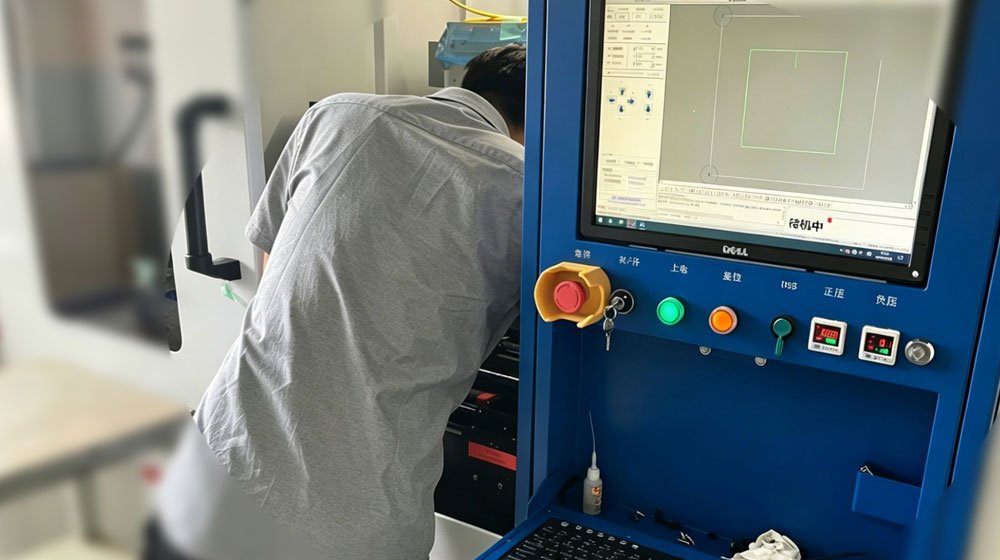
We once encountered a batch of AlN substrates whose edges turned yellow after laser cutting. After two days of troubleshooting, we confirmed that the laser power was too high, causing excessive thermal impact in the cutting area and ultimately resulting in yellow edges.
The problem was resolved by readjusting the relationship between laser power and cutting speed.
Therefore, laser parameters need to be tuned for each material and substrate thickness. A single set of parameters cannot be used to process all products. For a more detailed discussion of laser cutting principles, parameter selection, and common defects, see our guide to laser cutting of ceramic substrates.
For our high-end products, we currently use picosecond or femtosecond laser processing, with pulse widths of only 10⁻¹²–10⁻¹⁵ seconds. This results in lower thermal impact and better edge quality. However, this equipment is several times more expensive, so it is currently used only for our high-end product line.
Lapping and Polishing
After conventional cutting, the Ra surface roughness of the cut surface of some products is typically in the range of 0.5–1.0 μm. For applications with higher surface-quality requirements, lapping and polishing are used to control Ra within 0.1–0.3 μm, helping improve the bonding strength of the metallization layer and support long-term product reliability.
It is important to note:
- Insufficient lapping→ poor copper-layer adhesion
- Excessive lapping→ surface damage, reduced substrate strength, and more microcracks
Our internal comparison tests on specific products found that when the lapping removal amount increased from 0.05 mm to 0.15 mm, the flexural strength of the substrate decreased by approximately 10%–15%.
This shows that a smoother surface does not necessarily mean better performance.
For the products covered by this test, our control standard is to maintain the lapping removal amount within 0.05–0.08 mm while keeping Ra ≤0.3 μm.
Inspection and Quality Control for Ceramic Substrates
Before shipment, the following six items are subject to inspection:
| Inspection Item | Control Standard | Potential Impact |
| Dimensions (Length/Width) | Drawing tolerance ±0.1–0.2 mm | Affects subsequent placement, metallization, or module assembly |
| Thickness | Drawing tolerance ±0.05 mm | Uneven heat conduction and hot spots |
| Warpage | ≤0.1% for certain power module applications, depending on customer requirements | Poor metallization, placement deviation, incomplete soldering |
| Appearance | No scratches, foreign matter, or pores | Some appearance defects may indicate potential issues in forming, sintering, or machining |
| Edge Chipping | Chipping width ≤0.1 mm, depending on customer requirements | Severe chipping can become a source of stress concentration |
| Cracks | Zero tolerance | Crack propagation during thermal cycling → substrate fracture → module failure |
Most other defects mainly affect production yield, while cracks directly affect the structural reliability of the substrate. Therefore, we treat cracks as zero-tolerance defects.
We have established two inspection methods for screening cracks.
The first is transmitted-light inspection, which can detect most obvious cracks, pores, and internal abnormalities.
The second is ultrasonic scanning, which further identifies internal defects that may be difficult to detect through transmitted-light inspection.
Only products that pass both inspections are released for shipment.
How Manufacturing Processes Affect Ceramic Substrate Performance
The following table summarizes the key control parameters at each stage and their impact on final substrate performance:
| Process | Key Control Points | Consequences of Process Failure |
| Powder | Purity, oxygen content, particle-size distribution | Inadequate thermal conductivity, large batch-to-batch variation |
| Tape Casting | Green-body thickness and uniformity | Finished thickness deviation, inconsistent shrinkage |
| Debinding | Heating rate, atmosphere | Under severe process failure, AlN thermal conductivity may decrease significantly |
| Sintering | Temperature uniformity, atmosphere purity | Insufficient density, reduced thermal conductivity, excessive warpage |
| Flattening | Flatness, pressure profile | Excessive warpage → poor metallization → low assembly yield |
| Laser Cutting | Power/speed/focus matching | Edge chipping, microcracks, yellowing of AlN edges |
| Lapping | Material removal, final Ra value | Poor bonding if insufficient; reduced strength if excessive |
| Inspection | Full coverage of dimensions/warpage/cracks | Defects reaching the customer → complaints and returns |
Frequently Asked Questions
Q1: Which is more suitable for power module substrates, tape casting or dry pressing?
A1: For most thin power module substrates, tape casting offers greater advantages. It can produce thinner green bodies while providing better thickness uniformity and better surface quality.
Q2: What are the main causes of warpage in ceramic substrates?
A2: Ceramic substrate warpage mainly results from uneven shrinkage and residual stress during forming and sintering, as well as insufficient accuracy in subsequent flattening processes.
Power modules typically require substrate warpage of ≤0.1%. We control warpage through high-temperature pressure flattening combined with 100% laser inspection.
Q3: How does sintering affect ceramic substrate performance?
A3: The sintering process directly determines the final density, thermal conductivity, and mechanical strength of the ceramic substrate.
Changes in sintering temperature, atmosphere, and holding time can all affect the final performance of the substrate. These effects are particularly significant for products that are sensitive to material properties and dimensional accuracy.
Q4: How can you evaluate the technical capability of a ceramic substrate manufacturer?
A4: You can focus on the following key indicators:
- Powder source:For AlN, ask the supplier to provide an oxygen-content report.
- Sintering furnace:Check temperature uniformity and production stability across batches. You can ask the supplier to provide furnace temperature-uniformity test data.
- Crack inspection methods:Check whether both transmitted-light inspection and ultrasonic scanning are used.
- Batch-to-batch consistency:Ask the supplier to provide CPK data for consecutive batches and pay attention to both the CPK level and its stability across batches.
Conclusion
Bare ceramic substrates are not standardized components. They are a direct reflection of a manufacturer’s ability to integrate and control multiple manufacturing processes.
Even with the same drawing and the same raw material, products manufactured by different suppliers can show significant differences in performance.
These differences do not come from one particular “special trick” in any single process. Instead, they are hidden in the details of every manufacturing step—whether every powder batch is fully inspected, whether the debinding curve is monitored in real time, how well sintering temperature fluctuations are controlled, and what crack-detection methods are used.
These differences in process control may ultimately be reflected in the long-term reliability and service life of the modules.
If you are evaluating ceramic substrates for your application, you can also explore our ceramic substrate manufacturing capabilities or contact us to discuss your specific material, dimensional, and process requirements.