
Introduction
What Is a Ceramic Substrate? A ceramic substrate provides electrical insulation and heat dissipation in electronic circuits that require both functions. Engineers commonly use ceramic substrates in power modules and semiconductor packaging where thermal stability and reliability are critical.
Designers typically choose ceramic substrates when FR4 can no longer meet thermal management and reliability requirements. In SiC modules, heat is concentrated in the switching region close to the chip. Poor heat spreading directly accelerates thermal fatigue at the solder interface.
However, FR4 tends to warp and lose thermal stability at elevated temperatures. Thermal cycling stress first accumulates at the solder interface due to CTE mismatch. As a result, lower CTE mismatch between ceramic and copper reduces thermal stress in the joint. Alumina is still widely used in cost-sensitive industrial applications.
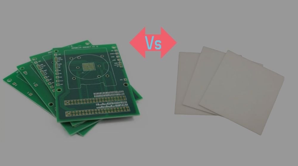
The contrast is clear when compared with FR4 used in low-power designs.
FR4 PCB vs Ceramic Substrate
| Item | FR4 PCB | Ceramic Substrate |
| Thermal Performance | Relatively low | Much higher |
| Thermal Conductivity | 0.3–0.5 W/m·K | 20–180 W/m·K |
| High-Temperature Resistance | Moderate | Excellent |
| Thermal Cycling Reliability | Limited | More stable |
| Electrical Insulation | Good | Excellent |
| Suitability for High-Power Applications | Limited | Better suited |
| Typical Applications | Consumer electronics | Power modules, EVs, SiC devices |
Therefore, the limitations of FR4 become more critical as power density increases in modern electronic systems.
Why Ceramic Substrates Are Irreplaceable?
Ceramic substrates provide both electrical insulation and heat dissipation, which is why they are used in power electronics and semiconductor packaging.
Reduced thermal stress improves solder joint and package reliability.
Automotive electronics and power modules rely on ceramic substrates when thermal cycling limits reliability.
Material selection defines how the substrate will perform under thermal and mechanical constraints.
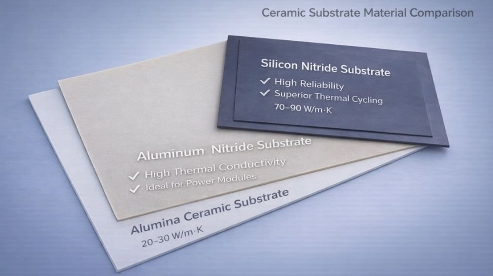
Common Ceramic Substrate Materials
Different ceramic materials show clear differences in thermal, mechanical, and cost behavior.
In practice, material selection is not driven by thermal conductivity alone.
Instead, reliability, machining feasibility, and production yield usually become the deciding factors in real applications.
The final choice is a trade-off between performance and manufacturability.
| Material | Thermal Conductivity | Strength | Cost | Typical Applications |
| Alumina (Al₂O₃) | Medium | Good | Low | General electronics |
| Aluminum Nitride (AlN) | High | Medium | High | Power modules |
| Silicon Nitride (Si₃N₄) | High | Excellent | High | EV modules |
| BeO | Very High | Medium | High | Special RF systems |
| Zirconia | Low | Excellent | Medium | Structural parts |
| ZTA | Medium | Very High | Medium | Wear-resistant parts |
Alumina (Al₂O₃)
Alumina is still the default choice for cost-driven and high-volume production.
It is less sensitive to process variation than AlN and Si₃N₄, which makes it suitable for industrial applications where consistency is more important than thermal performance.
Aluminum Nitride (AlN)
Engineers select AlN for high-power-density and SiC modules when thermal dissipation becomes the primary challenge.
For example, powder purity and oxygen content during sintering strongly affect thermal conductivity. Consequently, yield stability becomes more sensitive to process variation than in alumina substrates. Especially in large-area substrates.
Silicon Nitride (Si₃N₄)
Automotive power module designers choose Si₃N₄ when mechanical strength and crack resistance become critical.
Specialized Ceramic Materials
Most ceramic substrate applications use Al₂O₃, AlN, or Si₃N₄. Designers generally reserve BeO, ZTA, and SiC for applications with specific thermal, mechanical, or environmental requirements.
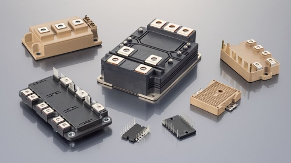
In most power module designs, manufacturers rarely use ceramic materials in bare form and typically combine them with metallization structures.
Ceramic Substrate Metallization Technologies
Two substrates made from the same ceramic may still behave very differently after brazing, especially when the copper structure or bonding process changes. As current increases, the copper layer and ceramic interface usually become one of the primary stress areas inside the module.
Bare Ceramic Substrates
Some applications only need the ceramic itself without a conductive layer. Manufacturers often machine these bare substrates later or use them directly as insulating parts.
Metallized Ceramic Substrates
Most power modules cannot use bare ceramic directly. A conductive layer still needs to be built on the surface for soldering and circuit connection. As a result, the copper interface often becomes one of the first failure points during thermal cycling.
DBC Substrates
DBC is still the most common structure in many power modules because thick copper can carry much higher current. In large IGBT modules, current load is usually not the biggest problem for DBC. Thermal stress near the copper edge is. Once copper thickness goes up, the stress after repeated thermal cycling becomes much harder to control, especially on larger substrates. As copper thickness increases, current carrying capability improves, but thermal stress at the copper-ceramic interface also rises.
DPC Substrates
When circuit spacing becomes very small, standard DBC processing is often no longer enough. This is where DPC starts becoming useful. LED packaging and small sensor modules often need much finer line width than thick copper structures can provide.
AMB Substrates
Automotive Si₃N₄ module manufacturers increasingly adopt AMB technology, mainly because bonding reliability is usually better under long-term thermal cycling.
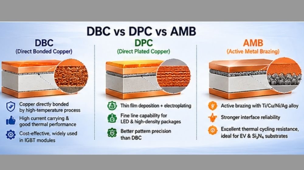
Compared with standard DBC, the copper layer is less likely to separate from the ceramic after repeated temperature changes.
The process, however, is also more sensitive. Small variations during brazing can affect yield quite noticeably.
HTCC and LTCC are more common in compact electronic packages where multiple circuit layers need to be integrated into a very small space. In RF and high-frequency devices, conventional substrate structures are often difficult to scale down further.
Once the material and metallization structure are defined, the next critical factor is how consistently the substrate can be manufactured.
Ceramic Substrate Manufacturing Process
A typical ceramic substrate production process includes:
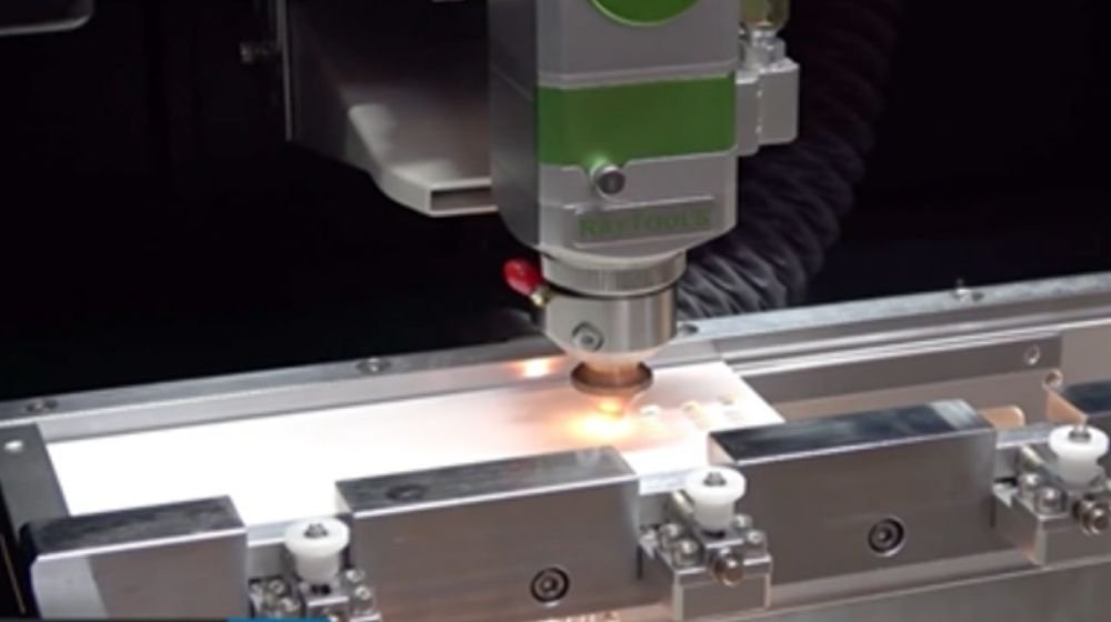
Raw Material Preparation → Forming → Sintering → Metallization → Laser Machining → Inspection
In reality, maintaining production consistency is often harder than achieving good laboratory results.
This is because sintering largely determines substrate density and thermal conductivity.
Meanwhile, metallization quality becomes increasingly important during thermal cycling. Once the metal-ceramic bond weakens, delamination or solder fatigue may appear.
In addition, large substrates are generally more sensitive to warpage after brazing, which can create assembly issues in high-power modules.
With AlN substrates, small density variations can already produce noticeable differences in thermal performance.
Key Ceramic Substrate Properties and Their Impact
| Parameter | Alumina(Al2O3) | Aluminum Nitride(AlN) | Silicon Nitride(Si3N4) | Impact on Performance |
| Thermal Conductivity | 20–30 W/m·K | 170–230 W/m·K | 70–95 W/m·K | Affects heat dissipation and chip temperature stability |
| Dielectric Strength | 12–18 kV/mm | 15–20 kV/mm | 12–18 kV/mm | Influences high-voltage insulation reliability |
| CTE | 6.5–7.5 ppm/K | 4.3–5.2 ppm/K | 2.8–3.5 ppm/K | Affects thermal stress and solder joint reliability |
| Surface Roughness (Ra) | 0.2–0.6 μm | 0.2–0.5 μm | 0.2–0.5 μm | Impacts metal adhesion and soldering quality |
| Flexural Strength | 300–400 MPa | 300–380 MPa | 600–800 MPa | Determines crack resistance and mechanical durability |
| Thermal Cycling Resistance | Medium | Good | Excellent | Affects long-term reliability under temperature changes |
| Flatness | Good | Good | Excellent | Influences mounting accuracy and assembly stability |
| Thickness Tolerance | ±0.03–0.08 mm | ±0.02–0.05 mm | ±0.02–0.05 mm | Affects processing precision and production consistency |
In real module design, thermal conductivity alone is not a deciding factor.
Thermal stress, crack resistance, flatness, and process stability directly affect reliability and yield in module assembly.
However, higher thermal conductivity improves heat dissipation but does not guarantee long-term reliability.
For this reason, engineers must carefully evaluate CTE mismatch, warpage, and metallization stress.
Therefore, design trade-offs often become more important than single-material performance at higher power densities.
Substrate reliability comes from balancing performance, manufacturability, and long-term stability.
Process variation directly determines field performance of ceramic substrates.
Typical Applications of Ceramic Substrates
EV Power Modules
For example, EV modules rarely operate at a stable temperature for long periods. EV modules rarely stay at a stable temperature for long. Fast charging and repeated acceleration usually create much more thermal cycling than traditional industrial systems. Frequent charging and acceleration cycles create repeated temperature fluctuations that place continuous mechanical stress on substrate structures and bonding interfaces.
IGBT Modules
Similarly, heat and current in large IGBT modules are often concentrated in a relatively small area. In larger IGBT modules, heat and current are both concentrated in a relatively small area. This is one reason DBC and AMB are still used so widely.
SiC Power Devices
Furthermore, heat no longer spreads evenly in many SiC modules as switching frequency increases. In many SiC modules, heat no longer spreads evenly once switching frequency starts increasing. The substrate quickly becomes one of the main thermal bottlenecks.
LED Packaging
Likewise, heat often accumulates near the chip area in high-power LED packages. In high-power LED packages, heat often accumulates directly near the chip area. Once junction temperature rises too much, brightness degradation becomes obvious quite quickly.
RF and Microwave Applications
At higher frequencies, signal loss becomes much more sensitive to substrate material. This is where ceramic structures still have a clear advantage.
Aerospace and Medical Devices
In aerospace and medical equipment, temperature fluctuation and long operating cycles usually leave very little margin for substrate deformation or cracking.
Industrial and Renewable Energy Systems
Some industrial inverters may run continuously for years with very limited cooling margin. Once heat starts accumulating inside the module, long-term reliability usually drops much faster than expected.
Manufacturing and Customization Considerations
In actual production, process stability and yield consistency influence material selection as much as thermal performance. Different ceramic substrate manufacturers may offer different metallization capability, substrate size range, flatness control, and thermal cycling reliability. For custom ceramic substrates used in power modules or EV systems, stable process control and large-scale manufacturing consistency are often more important than achieving the highest theoretical material performance.
Why Manufacturers Choose JingHui for Ceramic Substrates
| Ceramic Materials | Al₂O₃ / AlN / Si₃N₄ | ||
| Capability | Typical Options | ||
| Ceramic Materials | Al₂O₃ / AlN / Si₃N₄ | ||
| Substrate Structures | Bare Ceramic / DBC / DPC | ||
| Metallization Capability | Cu / MoMn / Ni-Au | ||
| Customization | Dimensions / Thickness / Layout | ||
| Manufacturing Support | Prototype & Volume Production | ||
| Applications | EV / IGBT / SiC / LED | ||
In real engineering projects, supplier capability often becomes a deciding factor once material options are narrowed down.
For engineering projects, manufacturing consistency, flatness control, metallization capability, and process stability are often as important as material specifications when evaluating ceramic substrate suppliers. Engineering teams typically evaluate these factors during design reviews,because laboratory material data alone rarely predicts long-term manufacturing performance.
Future Trends in Ceramic Substrates
As SiC and GaN devices become more common, demand for substrates with high thermal conductivity, high strength, and strong thermal cycling performance continues to grow.
According to Fraunhofer research and technical publications from leading power semiconductor manufacturers, the adoption of high-reliability ceramic substrates is accelerating alongside the growth of advanced power electronics. The use of AMB and Si₃N₄ substrates in EV applications is also expanding rapidly.
Ceramic Substrate FAQs
1.Why are Si3N4 substrates increasingly used in EV power modules?
EV manufacturers increasingly adopt Si3N4 substrates in power modules,because they provide excellent thermal cycling reliability and strong crack resistance. In automotive-grade power systems, substrates must withstand continuous heating, cooling, vibration, and high electrical loads over long operating periods.
Although AlN offers higher thermal conductivity, Si3N4 delivers better mechanical strength and fracture toughness. This helps reduce substrate cracking, solder fatigue, and copper delamination during repeated thermal cycling. For many EV manufacturers, long-term reliability is often more important than achieving the highest thermal conductivity alone.
2.What is the main difference between DBC and AMB substrates?
The biggest difference between DBC and AMB substrates is the copper bonding process. DBC substrates use oxide eutectic bonding, while AMB substrates use active metal brazing to join copper and ceramic materials.
In high-power applications such as IGBT and EV power modules, interface reliability becomes critical under repeated thermal cycling. AMB structures usually provide better bonding reliability and stronger crack resistance than traditional DBC structures. Because of this, AMB technology is becoming more common in Si3N4 automotive power modules and high-reliability electronic systems.
3.Why does higher thermal conductivity not always mean higher reliability?
Higher thermal conductivity improves heat dissipation, but many electronic failures are actually caused by thermal stress instead of overheating alone. In power modules, materials with poor CTE matching can create strong internal stress during repeated heating and cooling cycles.
Even when a substrate transfers heat efficiently, thermal expansion mismatch may still cause chip cracking, solder fatigue, or copper layer delamination. In real engineering applications, balanced thermal, mechanical, and electrical performance is usually more important than thermal conductivity alone.
4.Why do ceramic substrates crack?
Thermal expansion mismatch causes most ceramic substrate cracks, stress concentration, or manufacturing defects. In high-power electronics, repeated thermal cycling gradually increases stress between ceramic materials, copper layers, chips, and solder joints.
Over time, this stress can lead to ceramic cracking, interface separation, or solder fatigue failure. Poor Consequently, this stress can eventually lead to ceramic cracking sintering quality, unstable metallization processes, and insufficient flatness control can also increase crack risk during mass production.
5.Why are AlN substrates more expensive than Al2O3 substrates?
AlN usually looks attractive on paper because of its thermal conductivity, but production is much less forgiving than alumina once volume manufacturing starts. Small changes during sintering can affect AlN thermal conductivity quite noticeably, especially when oxygen control is unstable.
Once substrate size becomes larger or thickness gets thinner, AlN yield often starts fluctuating much more than alumina. Large AlN substrates may still pass laboratory testing, but keeping flatness and yield stable during mass production is usually harder. Processing steps such as laser cutting and metallization also become more sensitive on AlN, especially after brazing or thermal cycling tests.
6.Why is substrate flatness important?
If the substrate starts warping, solder thickness usually becomes uneven first. Problems during die bonding often appear soon after. In larger power modules, even slight warpage can leave some chip areas with much thicker solder than others. Heat then starts accumulating locally during operation.
Automatic die bonding equipment is usually much less tolerant of substrate warpage than manual assembly. Once flatness starts drifting, assembly yield usually drops first. Long-term thermal cycling problems often appear later. In automated production lines, flatness issues are often detected during die bonding long before they become visible during final inspection.
How to Select a Ceramic Substrate
Ceramic substrate selection should be based on actual operating conditions rather than thermal conductivity alone. In power electronics, different applications require different balances between thermal performance, mechanical reliability, manufacturing complexity, and cost control.
| Application Scenario | Recommended Solution |
| Cost-sensitive applications | Al₂O₃ substrates |
| High thermal conductivity requirements | AlN substrates |
| High reliability EV systems | Si₃N₄ substrates |
| Fine circuit patterns | DPC substrates |
| High current applications | DBC substrates |
| Strong thermal cycling reliability | AMB substrates |
For general industrial electronics and consumer applications, Al₂O₃ remains the most widely used option because of its mature manufacturing process and relatively low cost. In high-power systems with high heat density, AlN substrates provide much better thermal conductivity and are commonly used for power module substrate selection.
For EV ceramic substrate selection, long-term reliability under vibration and thermal cycling is often more important than achieving the highest thermal conductivity. Because of this, Si₃N₄ substrates are increasingly used in automotive-grade power modules due to their superior fracture toughness and crack resistance.
DBC vs AMB selection mainly depends on current capability and reliability requirements. DBC structures are widely used because of their mature supply chain and strong current carrying capability, while AMB substrates are often preferred in high-reliability SiC and EV applications where thermal cycling performance is critical.
AlN vs Si₃N₄
AlN is mainly used when thermal dissipation is the priority.
Si₃N₄ is chosen when mechanical strength and thermal cycling resistance become limiting factors, especially in automotive environments.
How to Evaluate a Ceramic Substrate Supplier
Material data is only part of the evaluation.
Process consistency, flatness control, and metallization quality usually have more impact on yield than nominal properties.
Common Selection Mistakes
Thermal conductivity is often over-emphasized in early design stages.
In practice, thermal stress and crack behavior usually dominate long-term failure modes.
Manufacturing capability is another overlooked factor. Some materials behave well in lab tests but become unstable in large-format or high-volume production.
Conclusion
Ceramic substrates are widely used in power electronics, semiconductor packaging, and other applications where thermal management and reliability are critical. The most suitable substrate is not always the one with the highest specification. Application requirements, manufacturing constraints, and long-term reliability targets often determine the final choice.
Need Help Selecting the Right Ceramic Substrate?
A drawing and basic operating conditions are usually enough for initial evaluation. Material selection can then be narrowed based on thermal load and reliability targets. Our engineering team can assist with ceramic material selection, DBC/AMB structure recommendations, flatness requirements, metallization options, and manufacturability assessment for both prototype and volume production projects.