

Introduction
Ceramic substrate warpage is one of the most common flatness issues in power electronics packaging. A substrate may pass incoming inspection, yet excessive warpage can still develop during reflow soldering or long-term service.
Warpage behavior is closely related to substrate structure and material selection. For an overview of ceramic substrate materials and applications, see our ceramic substrates for power electronics. The fundamentals of substrate types, materials, and manufacturing are covered in our ceramic substrate guide.
Based on our manufacturing experience, warpage-related issues have contributed to approximately 15–20% of packaging defects in certain power module projects. Rather than being an isolated quality issue, warpage is typically caused by accumulated stresses throughout material selection, structural design, and manufacturing processes.
This article explains ceramic substrate warpage from an engineering perspective, covering its formation mechanisms, measurement methods, industry standards, and practical strategies for minimizing warpage in production.
What Is Ceramic Substrate Warpage
Ceramic substrate warpage refers to the deformation of a ceramic substrate away from its intended flat plane. In simple terms, the substrate is no longer perfectly flat.
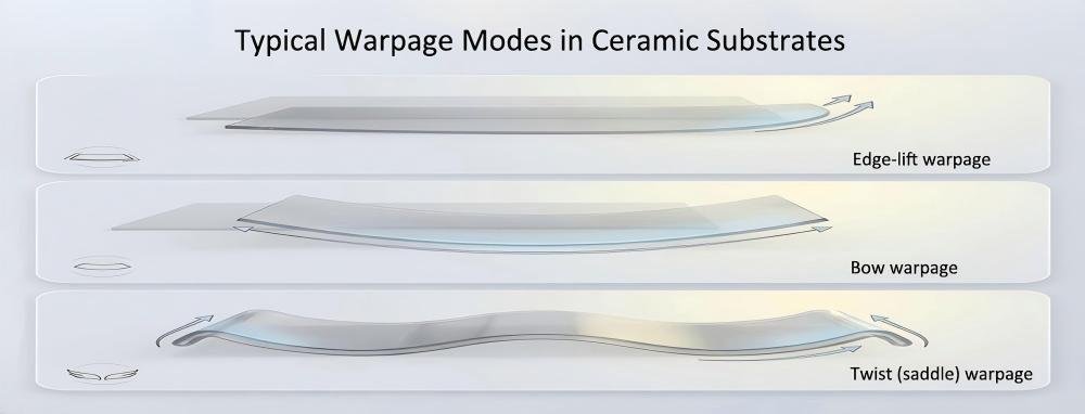
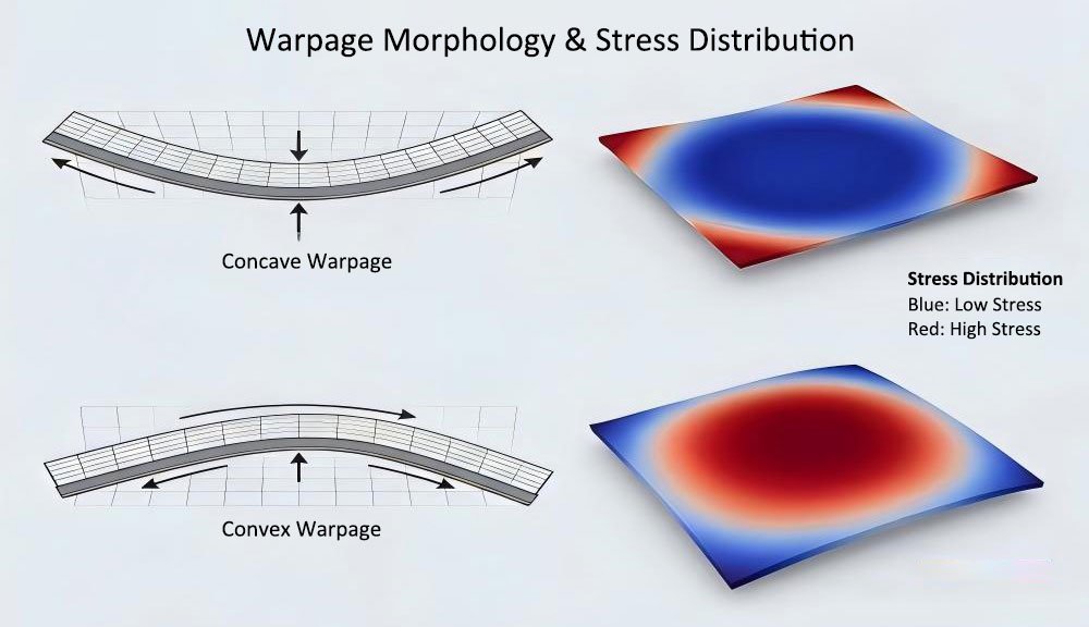
From a mechanical standpoint, warpage occurs when residual stresses within the substrate exceed the material’s ability to maintain dimensional stability. Depending on the stress distribution, ceramic substrate warpage generally appears in two forms:
Bow Warpage
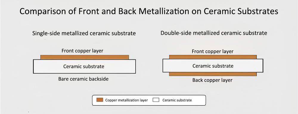
Bow warpage is a one-directional curvature in which the center of the substrate bends upward or downward. It is typically caused by asymmetric stresses between the top and bottom surfaces, such as unequal copper thickness or metallization coverage.
Twist Warpage (Saddle Warpage)
Twist warpage produces a saddle-shaped deformation, with opposite corners displaced in different directions.
This type of warpage is generally more difficult to correct than bow warpage. During SMT (Surface Mount Technology) assembly, severe twisting can prevent vacuum nozzles from picking up the substrate properly, resulting in machine alarms, placement errors, or even scrapped parts.
The fundamental principle of warpage control is straightforward: maintain a symmetrical stress distribution and release residual stresses whenever possible.
In addition to bow and twist warpage, edge-lift warpage may also occur in ceramic substrates. It is typically caused by localized stress imbalance near the edges and is less common but still relevant in asymmetric metallization structures.
What Causes Ceramic Substrate Warpage?
Ceramic substrate warpage rarely results from a single factor. In most cases, it develops from the combined effects of material characteristics, manufacturing processes, and operating conditions.
Residual Stress in Materials
1. Ceramic Powder Quality
The quality of the ceramic powder has a direct impact on the internal stress of the substrate.
A broad particle size distribution or insufficient powder purity can increase the likelihood of pores forming during sintering. These pores act as stress concentration sites, making the substrate more susceptible to deformation.
2. Coefficient of Thermal Expansion (CTE) Mismatch
Another major source of warpage is the difference in the coefficient of thermal expansion (CTE) between the ceramic and the metallization layer.
For example, alumina has a CTE of approximately 7 ppm/°C, while copper is about 17 ppm/°C. As the temperature changes, the copper and ceramic expand and contract at different rates, generating thermal stresses at the interface.
Although this CTE mismatch cannot be eliminated, its impact can be significantly reduced through symmetrical structural design.
In addition, a large difference in copper thickness between the top and bottom surfaces can greatly increase the risk of warpage. In one project discussed later in this article, a substrate with 0.30 mm copper on one side and 0.10 mm on the other reached 190 μm of warpage after reflow soldering, resulting in an 8% placement reject rate.
Process-Related Defects
Manufacturing processes can either relieve residual stress or introduce additional stress into the substrate.
A more detailed breakdown of how each manufacturing step influences stress evolution is provided in the ceramic substrate manufacturing process.
1. Excessive Heating or Cooling Rates
If the heating or cooling rate is too fast, especially during the high-temperature stage of sintering, the temperature difference between the surface and the core becomes excessive.
For example, when the cooling rate exceeds 10°C/min, the internal temperature gradient may exceed 50°C. Under these conditions, thermal stresses can become “locked” inside the substrate before they have time to relax.
2. Improper Binder Burnout
During binder burnout, heating too quickly (typically above 5°C/min) may cause organic binders to decompose too rapidly.
This can leave microscopic cracks or internal defects that are often invisible after sintering but later contribute to warpage or reliability problems.
3. Forming Defects
Variations in green sheet thickness can also lead to warpage.
When tape casting thickness fluctuates by more than ±10 μm, different areas shrink unevenly during sintering, generating residual stress.
Similarly, insufficient cold isostatic pressing (CIP) pressure can produce non-uniform green density, resulting in uneven shrinkage and increased deformation after sintering.
Service Environment
Power modules operate under continuously changing thermal conditions rather than static environments.
Repeated thermal cycling between −40°C and 150°C, high-frequency power fluctuations, and thermal shock gradually accumulate residual stresses over time.
As these stresses build up through repeated operating cycles, ceramic substrate warpage may progressively increase, even if the substrate initially met flatness requirements.
Ceramic Substrate Warpage Measurement
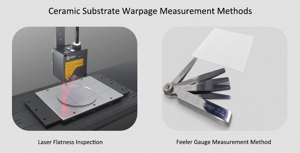
Warpage is generally defined as the maximum deviation of the substrate surface from a reference plane. It can be expressed either as an absolute value (μm) or as a percentage of the substrate diagonal length (%).
One fundamental rule applies to every measurement method:
The substrate must be supported in a free, unstressed condition without applying any external force to flatten it.
| Measurement Method | Typical Accuracy | Typical Applications | Key Features |
| Feeler Gauge | ±10 μm | Incoming inspection and quick sampling | Measures only the maximum gap at a single point; cannot distinguish bow from twist |
| Laser Profilometer (3D Scanning) | ±2 μm | High-volume production and full inspection | Generates a full 3D surface profile, enabling accurate identification of warpage type |
| Confocal Microscope | ±0.5 μm | Laboratory analysis and failure investigation | Highest measurement accuracy but relatively slow, making it unsuitable for production lines |
| Dynamic Warpage Testing | ±5 μm | Automotive and optical communication applications | Monitors warpage continuously from room temperature to 260°C, revealing high-temperature deformation that static measurements cannot detect |
Best Practices for Warpage Measurement
To obtain reliable and repeatable results, several factors should be controlled during measurement:
- Maintain an ambient temperature of 23 ± 2°C and relative humidity between 40% and 60%.
- Support the substrate using a three-point ball supportto minimize deformation caused by gravity.
- For bow warpage, calculate the total absolute displacement between the highest and lowest points.
- For twist warpage, use the maximum deformation measured along the diagonal direction.
One important consideration for dynamic warpage testing is that the heating and cooling profile should closely match the customer’s actual reflow soldering profile. Otherwise, the measured results may not accurately reflect real operating conditions.
Which Ceramic Materials Are More Sensitive to Warpage?
In practical engineering, the ceramic material itself does not directly determine whether warpage will occur. However, material choice plays an important role in how sensitive a substrate is to design and process variations.
For a deeper comparison of thermal, mechanical, and cost-related trade-offs between these materials, see Al₂O₃ vs AlN vs Si₃N₄: which is best for power modules?
In general, the three most common ceramic materials used for power modules exhibit different warpage characteristics:
- Alumina (Al₂O₃): The most stable and mature ceramic system. It is relatively tolerant of process variations, although asymmetric structures can still result in predictable warpage.
- Aluminum Nitride (AlN): Offers excellent thermal conductivity but is more sensitive to sintering and cooling conditions. As a result, batch-to-batch variations are more likely to produce inconsistent warpage.
- Silicon Nitride (Si₃N₄): Provides outstanding mechanical strength and fracture resistance. However, in multilayer structures such as AMB substrates, the interfacial stress distribution is more complex, making dimensional changes during thermal cycling more pronounced.
In practice, differences in warpage are influenced far more by structural design and manufacturing processes than by the ceramic material alone.
Industry Standards and Acceptance Criteria for Ceramic Substrate Warpage
At present, there is no universally accepted standard specifically for ceramic substrate warpage. Different industries and manufacturers typically adopt their own acceptance criteria based on product reliability requirements.
| Standard / Specification | Warpage Limit | Additional Requirements | Typical Applications |
| IPC-6012 (commonly used as a PCB industry reference) | ≤0.75% of substrate diagonal | Static measurement at room temperature | General electronics |
| Typical automotive customer specifications | ≤0.5% of substrate diagonal | Dynamic warpage data from room temperature to 260°C required | Automotive power modules |
| Optical communication industry | Typically <30 μm (absolute value) | Often requires verification at 150°C | Optical modules and high-speed interconnects |
| Internal specifications of leading power module manufacturers | ≤0.3–0.4% of substrate diagonal | Additional measurement at peak reflow temperature | IGBT and SiC power modules |
However, in real engineering applications, the numerical limit alone does not tell the whole story. Measurement results are only comparable when the following three conditions are consistent:
1. Measurement Temperature
A substrate that meets the flatness requirement at room temperature may still exceed the allowable warpage during reflow soldering or under high-temperature operating conditions.
2. Measurement Method
The measurement method can significantly affect the reported result.
For example, three-point support and best-fit plane (full-surface fitting) may produce values that differ by 10–20 μm for the same substrate.
3. Warpage Definition
Warpage values also depend on how they are calculated.
For example:
- How is bow warpagedefined?
- How is twist warpagecalculated?
- Is the reference plane established using three-point supportor a best-fit plane?
If these conditions are not aligned, comparing numerical warpage values becomes meaningless, regardless of how strict the specified limit may be.
How to Control Ceramic Substrate Warpage in Engineering
The key to controlling ceramic substrate warpage is simple: minimize the generation of residual stress and release the stress that cannot be avoided.
Based on our engineering experience, effective warpage control should begin during the design stage and continue throughout the entire manufacturing process.
Design for Warpage Control
Many warpage problems are actually designed into the substrate long before manufacturing begins. The following design guidelines have proven effective in reducing warpage risk.
1. Copper Thickness
For DBC ceramic substrates, the copper thickness on each side is generally recommended to be no more than approximately 15% of the ceramic thickness.
For example, on a ceramic substrate with a thickness of 0.38 mm, the copper thickness on one side should ideally not exceed 0.057 mm.
Excessively thick copper layers generate higher thermal stresses during heating and cooling, increasing the likelihood of warpage.
2. Symmetrical Metallization Coverage
The difference in metallization coverage between the top and bottom surfaces should generally be kept within 30%.
If one side requires a large copper area for electrical or thermal performance, adding a dummy copper layer on the opposite side can help balance the stress distribution.
3. Ceramic Thickness
Thin ceramic substrates are inherently more susceptible to deformation.
When the substrate thickness is less than 0.32 mm, a dedicated warpage assessment is recommended during the design stage.
4. Additional Considerations for AMB Substrates
Compared with DBC substrates, AMB (Active Metal Brazed) substrates contain an additional brazing layer that introduces extra interfacial stress.
For this reason, the recommended copper thickness ratio is typically reduced to 12% or less of the ceramic thickness.
Optimize the Sintering Process
The cooling profile during sintering has a significant influence on residual stress.
For temperatures above 1000°C, the cooling rate is typically recommended to remain between 5 and 8°C/min and should not exceed 10°C/min.
Faster cooling creates larger temperature gradients between the surface and the interior of the substrate, increasing the amount of residual thermal stress retained after sintering.
Do Not Skip the Annealing Process
After metallization or electroplating, an annealing treatment at 250–300°C for 1–2 hours helps relieve newly introduced interfacial stresses.
Although some manufacturers omit this step to reduce production costs or energy consumption, doing so can significantly increase the risk of warpage.
In one of our comparative production trials, substrates that did not undergo annealing exhibited more than twice the high-temperature warpage of annealed substrates manufactured from the same production batch.
Control Forming and Raw Materials
Consistent forming quality and stable raw materials are equally important for minimizing warpage.
Recommended control measures include:
- Keep tape-casting thickness variation within ±10 μm.
- Verify the consistency of every incoming powder batch, particularly the D10, D50, and D90 particle size distribution.
- Apply sufficient cold isostatic pressing (CIP) pressure—typically above 200 MPa—to achieve uniform green density before sintering.
As demonstrated in Case Study 2, an increase in D90 from 3.2 μm to 7.8 μm caused severe warpage variation despite no changes to the production line or sintering process.
Quick Reference for Warpage Control
| Production Stage | Control Item | Recommended Target |
| Design | Copper thickness | ≤15% of ceramic thickness (per side) |
| Design | Metallization symmetry | Difference between top and bottom ≤30%; use dummy copper if necessary |
| Design | Ceramic thickness | Perform dedicated warpage evaluation when thickness is <0.32 mm |
| Sintering | Cooling rate | 5–8°C/min above 1000°C |
| Post-metallization | Annealing | 250–300°C for 1–2 hours |
| Forming | Tape-casting thickness | Variation within ±10 μm |
| Incoming inspection | Powder particle size | Inspect D10, D50, and D90 for every batch |
No single measure can eliminate ceramic substrate warpage. The best results are achieved by combining optimized design, stable raw materials, and well-controlled manufacturing processes throughout the entire production cycle.
Case Studies
Case 1: Asymmetrical Copper Layers Increased Warpage After Reflow Soldering
A DBC substrate consisted of a 0.38 mm Al₂O₃ ceramic with 0.30 mm copper on the top side and 0.10 mm copper on the bottom side.
At room temperature, the substrate exhibited a warpage of 45 μm, which met the customer’s inspection criteria. However, after reflow soldering, the warpage increased to 190 μm, resulting in an 8% component placement rejection rate.
The root cause was the 0.20 mm thickness difference between the top and bottom copper layers, which created severe thermal stress imbalance during heating.
Solution: The top copper thickness was reduced to 0.20 mm, while a 0.20 mm dummy copper layer was added to the backside to balance the stress.
After optimization:
- Room-temperature warpage decreased to 28 μm.
- Maximum warpage during reflow dropped to 45 μm.
- The placement rejection rate fell from 8% to 0.3%.
Summary: Symmetrical structural design is one of the most effective ways to reduce ceramic substrate warpage.
Case 2: Powder Batch Variation Caused Large Warpage Fluctuations
An AlN ceramic substrate manufactured on the same production line and in the same sintering furnace showed warpage ranging from 15 μm to 120 μm, resulting in a 40% rejection rate.
The investigation revealed that the ceramic powder supplier had changed batches. The D90 particle size increased from 3.2 μm to 7.8 μm, introducing more coarse particles and causing non-uniform green-body density before sintering.
Solution: The powder batch was replaced, and incoming quality control was upgraded to inspect D10, D50, and D90 for every batch.
After implementing these controls:
- Warpage stabilized between 30 μm and 50 μm.
- The process capability index (CpK) improved from 0.67 to 1.33.
Summary: If the incoming ceramic powder is unstable, downstream process optimization alone cannot eliminate warpage.
Note: These case studies are based on actual production projects at JH Ceramics. Some values have been anonymized, and actual results may vary depending on substrate dimensions, ceramic materials, copper patterns, and product design.
Frequently Asked Questions
Q1. Why does a ceramic substrate pass room-temperature inspection but warp after reflow soldering?
A1: Residual stress may remain dormant at room temperature. During reflow soldering, the difference in thermal expansion between the ceramic and copper layers generates additional thermal stress, causing the latent warpage to become apparent.
Q2. What level of warpage is considered acceptable?
A2: There is no universal standard. As a general reference:
- General electronics: ≤0.75%
- Automotive power modules: ≤0.5%
- Optical communication modules: typically <30 μm
More importantly, both supplier and customer should use the same measurement method and test temperature when evaluating warpage.
Q3. Will adding a dummy copper layer affect electrical performance?
A3: No. A dummy copper layer is not connected to the electrical circuit and carries no current.
As long as it is properly designed to avoid critical high-frequency signal areas, it has virtually no impact on electrical performance while significantly improving stress balance.
Q4. Is AlN more prone to warpage than Al₂O₃?
A4: Generally, yes. Aluminum nitride is more sensitive to thermal stress and offers a narrower process window than alumina.
However, its much higher thermal conductivity makes it the preferred material for many high-power applications. This is a classic engineering trade-off between thermal performance and manufacturing robustness.
Q5. Which is more difficult to control: bow warpage or twist warpage?
A5: Twist warpage. Bow warpage can often be reduced through process optimization, while twist warpage is much harder to correct.
In SMT assembly, severe twisting may prevent vacuum nozzles from picking up components properly, often leading to production stoppages or product rejection.
Q6. Is 100% outgoing inspection enough to ensure low warpage?
A6: No. Inspection only identifies defective parts—it does not prevent defects from occurring.
A capable supplier should control warpage throughout the manufacturing process, including powder consistency, sintering profiles, annealing conditions, and in-process monitoring.
Conclusion
Perfectly flat ceramic substrates do not exist. In practice, ceramic substrate warpage is a result of stress imbalance caused by material properties, structural design, and manufacturing processes.
The most effective way to minimize warpage is to address it early—during material selection, substrate design, and process development—rather than relying solely on final inspection.
A structured engineering approach to material and application selection is summarized in how to select the right ceramic substrate for power modules.
If you are developing ceramic substrates for power modules or experiencing warpage during SMT assembly or reflow soldering, our engineering team can help evaluate your design and recommend practical solutions to improve yield and long-term reliability.