

Introduction
Direct Bonded Copper (DBC) ceramic substrates are widely used in IGBT modules, SiC power modules, automotive electronics, renewable energy converters, railway traction systems, and industrial power equipment. Their combination of high current carrying capability, excellent thermal conductivity, and reliable electrical insulation makes them one of the most important substrate technologies for modern power electronics.
However, one failure mode continues to concern both manufacturers and design engineers—delamination.

Unlike visible ceramic cracking, delamination usually develops inside the copper-to-ceramic interface. It often begins as microscopic separation after repeated thermal cycling and gradually propagates under mechanical or thermal stress. As the bonded area decreases, thermal resistance increases, heat distribution becomes less uniform, and local hot spots begin to form. Eventually, electrical performance deteriorates, solder joints experience additional stress, and complete module failure may occur.
Many engineers initially suspect poor manufacturing quality whenever delamination is observed. In reality, interface separation is rarely caused by a single defect. Material properties, copper thickness, thermal expansion mismatch, manufacturing parameters, assembly design, and operating conditions all interact throughout the product life cycle.
Understanding these mechanisms is essential for improving long-term reliability rather than simply identifying failed products after testing.
What Is DBC Delamination?
DBC delamination refers to the partial or complete separation between the copper layer and the ceramic substrate after bonding.
Unlike ceramic fracture, the ceramic itself often remains intact while the bonded interface gradually loses adhesion. Because heat generated by power semiconductor devices must transfer through this interface, even a relatively small delaminated region can significantly reduce thermal performance.
Depending on stress distribution, delamination may begin at the edge of the substrate, near corners where stress concentrates, or directly beneath high-power semiconductor chips where repeated heating occurs.
Typical characteristics include:
- Partial copper lift-off
- Interfacial crack growth
- Increased thermal resistance
- Localized overheating
- Reduced mechanical strength
- Progressive reliability degradation
If not detected early, the damaged interface usually continues to propagate during subsequent thermal cycling.
Why Does DBC Delamination Occur?
DBC delamination is rarely caused by one single factor. Instead, it usually results from the interaction of thermal, mechanical, material, and manufacturing stresses accumulated over time.
1. Thermal Expansion Mismatch
Copper expands approximately two to five times more than common engineering ceramics during heating. During every heating and cooling cycle, the copper layer attempts to expand and contract more than the ceramic substrate.
Because both materials are permanently bonded together, this mismatch generates shear stress along the bonding interface. Although a single cycle may not create visible damage, thousands of cycles gradually initiate microscopic cracks that eventually develop into delamination.
This fatigue mechanism is one of the primary reasons why DBC reliability testing emphasizes thermal cycling rather than static mechanical loading.
2. Residual Stress After Bonding
During DBC manufacturing, copper is bonded onto ceramic at elevated temperatures under carefully controlled atmospheric conditions. As the assembly cools to room temperature, both materials shrink at different rates.
Even before the substrate enters service, residual stress already exists inside the interface. If process parameters such as bonding temperature, cooling rate, or copper thickness are not optimized, excessive residual stress may significantly reduce long-term reliability.
Residual stress itself may not immediately cause delamination, but it creates an initial stress condition that accelerates fatigue during later thermal cycling.
3. Poor Copper Bond Quality
The copper-to-ceramic interface is the most critical region of a DBC substrate. Even when both the ceramic and copper individually meet specification, poor interfacial bonding can significantly reduce long-term reliability.
During the DBC process, the copper layer forms a direct bond with the ceramic through a controlled high-temperature oxidation reaction. Stable bonding requires clean copper surfaces, proper oxidation control, uniform temperature distribution, and carefully managed process parameters. Any deviation can weaken the interface before the substrate is even placed into service.
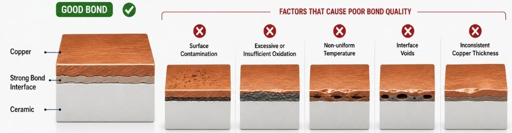
Common manufacturing issues include:
- Surface contamination before bonding
- Excessive or insufficient oxidation
- Non-uniform bonding temperature
- Local voids at the interface
- Inconsistent copper thickness
- Uneven surface flatness
These defects do not always cause immediate failure. Many substrates pass dimensional inspection and electrical testing but later develop interface separation after repeated thermal loading.
For this reason, interface quality should be evaluated not only by appearance, but also by bond strength, microstructure, and long-term reliability testing.
4. Thermal Cycling Fatigue
Thermal cycling is widely recognized as one of the primary causes of DBC delamination.
Power electronic devices rarely operate at a constant temperature. During normal operation, semiconductor chips repeatedly heat up under load and cool down after power reduction. Every temperature fluctuation generates expansion and contraction inside the bonded structure.
Although each individual cycle creates only a small amount of stress, the accumulated fatigue damage becomes significant after thousands of cycles.
Typically, the failure process develops in several stages:
- Residual stress already exists after manufacturing.
- Repeated thermal cycling generates microscopic interface cracks.
- Small cracks gradually connect and propagate.
- Local heat transfer becomes less efficient.
- Higher operating temperatures accelerate crack growth.
- Partial delamination develops into complete interface separation.
Once delamination begins, the degradation process often accelerates because increased thermal resistance produces even higher operating temperatures.
This positive feedback mechanism explains why many DBC substrates appear stable for long periods before experiencing rapid reliability deterioration.
5. Ceramic Material Selection
The ceramic material itself does not directly determine whether delamination will occur, but it strongly influences thermal stress, mechanical strength, and long-term fatigue resistance.
Different engineering ceramics exhibit different coefficients of thermal expansion, elastic modulus, fracture toughness, and thermal conductivity. These properties affect how stress is distributed throughout the DBC structure.
Typical Engineering Comparison
| Ceramic | Thermal Conductivity | Thermal Cycling Reliability | Relative Delamination Risk |
|---|---|---|---|
| Alumina (Al₂O₃) | Moderate | Good | Medium |
| Aluminum Nitride (AlN) | High | Very Good | Medium-Low |
| Silicon Nitride (Si₃N₄) | Medium | Excellent | Lowest |
Alumina remains the most economical solution for general industrial applications.
Aluminum nitride provides significantly better heat dissipation, making it suitable for high-power electronic modules.
Silicon nitride offers exceptional fracture toughness and thermal cycling resistance, making it increasingly attractive for demanding automotive power modules.
However, material selection should always consider cost, thermal performance, mechanical reliability, and manufacturing capability together rather than relying on a single property.
6. Mechanical Stress
Not all delamination originates from thermal cycling. External mechanical loading can also introduce significant stress into the bonded interface.
Typical sources include:
- Uneven heat sink surfaces
- Excessive mounting torque
- PCB deformation
- Package warpage
- Transportation vibration
- Mechanical shock
Even relatively small bending deformation may locally increase interface stress, especially near substrate corners and mounting holes.
Good mechanical design should distribute stress evenly throughout the module rather than concentrating it in localized regions.
Typical Delamination Modes
Although every application is different, most DBC interface failures can generally be classified into four typical modes.
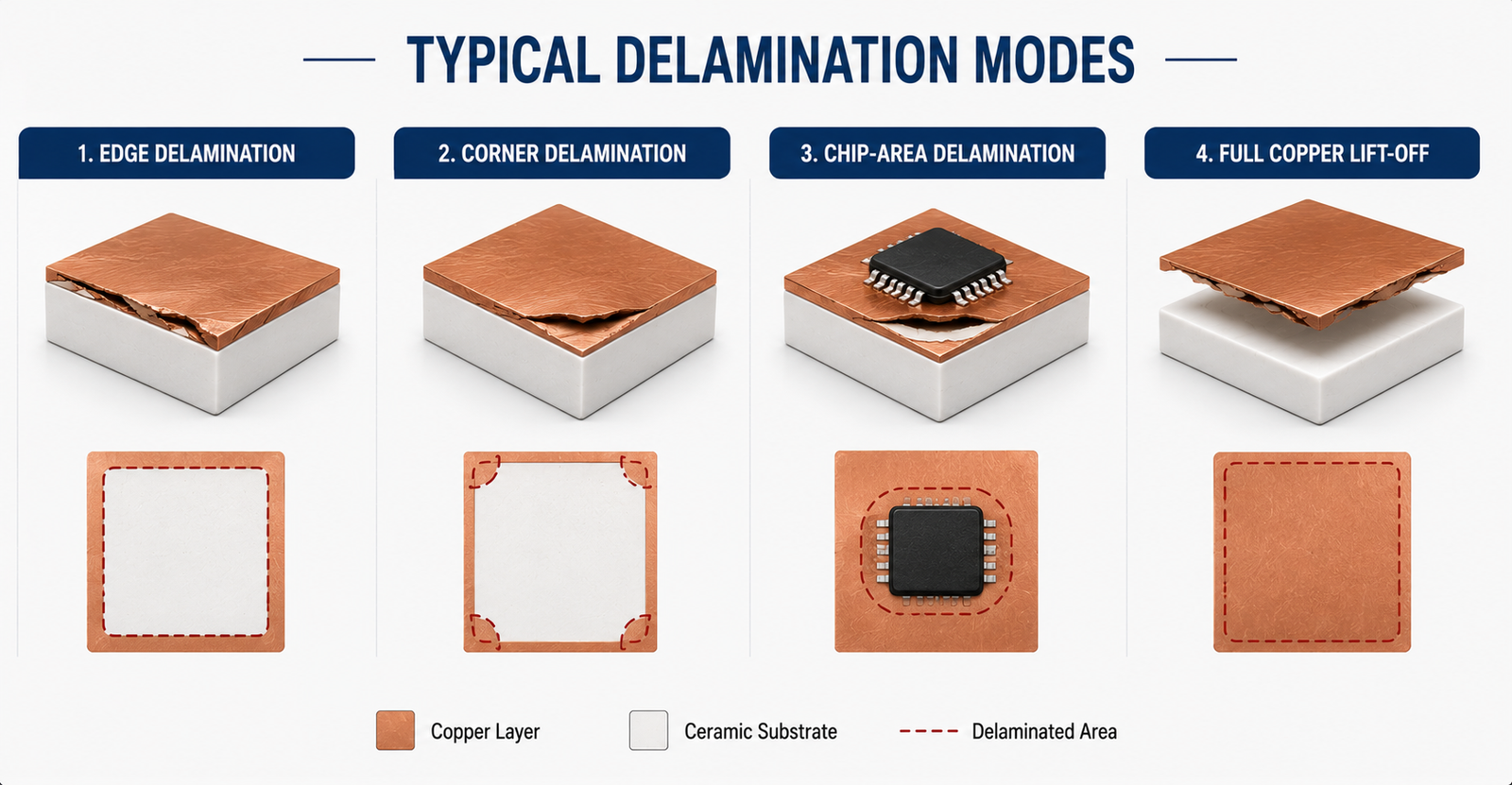
Edge Delamination
Delamination starts from the substrate edge where stress concentration is highest and gradually propagates toward the center.
Corner Delamination
Corners experience multi-directional stress during thermal expansion and contraction, making them particularly vulnerable to crack initiation.
Chip-Area Delamination
High heat flux beneath semiconductor chips accelerates local thermal fatigue, making the chip attachment region one of the most critical reliability areas.
Full Copper Lift-Off
In severe cases, large portions of the copper layer separate completely from the ceramic substrate, resulting in dramatic increases in thermal resistance and loss of mechanical integrity.
How Engineers Detect DBC Delamination
Because delamination usually begins inside the copper–ceramic interface, it is often invisible during routine visual inspection. A substrate may appear normal externally while significant interfacial separation has already developed internally.
For high-reliability applications such as electric vehicles, industrial inverters, railway traction systems, and aerospace electronics, manufacturers typically combine multiple inspection methods to evaluate interface integrity throughout product development and qualification.
No single inspection method is suitable for every situation. Engineers normally select different techniques depending on production stage, cost, required accuracy, and whether destructive testing is acceptable.
1. Scanning Acoustic Microscopy (SAM)
Scanning Acoustic Microscopy (SAM) is one of the most widely used non-destructive inspection methods for DBC substrates.
Ultrasonic waves travel differently through bonded and unbonded regions. When internal voids or delamination exist, part of the ultrasonic signal is reflected, allowing software to generate a detailed interface image.
SAM can detect:
- Interfacial voids
- Initial delamination
- Bonding defects
- Crack propagation
- Local debonding beneath copper
Because it does not damage the substrate, SAM is commonly used during product qualification and reliability verification.
2. Cross-Section Analysis
Cross-sectional metallographic analysis remains one of the most reliable methods for failure investigation.
After cutting, polishing, and microscopic observation, engineers can directly evaluate:
- Interface continuity
- Copper thickness
- Ceramic microstructure
- Oxide layer condition
- Crack initiation sites
Although destructive, cross-section analysis provides information unavailable through external inspection alone.
3. Thermal Resistance Monitoring
As delamination grows, thermal resistance increases because heat must bypass separated regions.
Many reliability laboratories monitor junction temperature or thermal impedance during thermal cycling tests. A gradual increase in thermal resistance often indicates progressive interface degradation before catastrophic failure occurs.
4. X-ray Inspection
Although X-ray imaging cannot clearly reveal every interfacial crack, it is useful for identifying:
- Large voids
- Package deformation
- Copper lifting
- Internal structural abnormalities
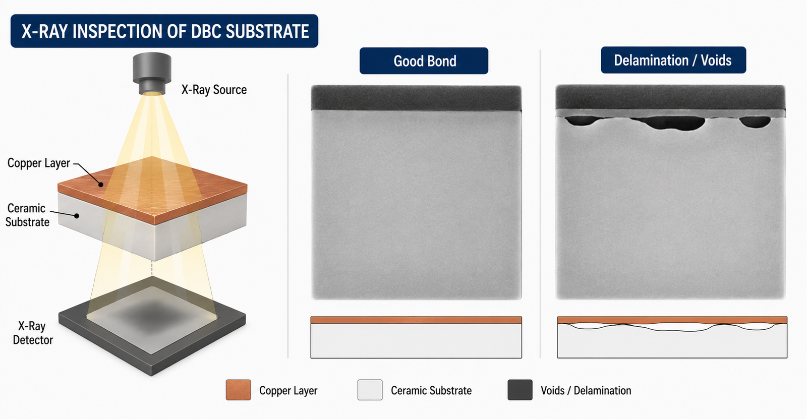
X-ray is frequently combined with SAM during comprehensive failure analysis.
How to Prevent DBC Delamination
Preventing delamination begins long before production starts. Material selection, structural design, manufacturing control, and application conditions all influence long-term interface reliability.
1. Select the Appropriate Ceramic Material
Different ceramic materials exhibit different thermal conductivity, fracture toughness, and thermal expansion characteristics.
Rather than selecting materials solely according to thermal conductivity, engineers should evaluate:
- Expected operating temperature
- Thermal cycling frequency
- Mechanical loading
- Lifetime requirements
- Cost targets
For high-power automotive modules, thermal cycling reliability often becomes more important than thermal conductivity alone.
2. Optimize Copper Thickness
Thicker copper increases current carrying capability but also generates higher thermal stress.
Engineers should balance:
- Electrical performance
- Heat spreading
- Residual stress
- Manufacturability
Excessively thick copper does not always improve reliability.
3. Improve Interface Quality
Stable bonding depends on consistent manufacturing.
Key process controls include:
- Surface cleanliness
- Oxidation control
- Furnace atmosphere
- Temperature uniformity
- Cooling rate
- Flatness control
Small process variations can significantly influence long-term bond strength.
4. Reduce Stress Concentration
Mechanical design should avoid unnecessary stress concentration.
Examples include:
- Smooth copper corners
- Uniform copper distribution
- Proper chip layout
- Symmetrical structures
- Controlled mounting force
Reducing localized stress often provides greater reliability improvement than increasing material strength alone.
Engineering Design Recommendations
Successful DBC reliability depends on system-level optimization rather than any single material property.
Design Checklist
✔ Select ceramic material according to application environment.
✔ Avoid unnecessary copper thickness.
✔ Maintain uniform heat distribution.
✔ Reduce edge stress concentration.
✔ Optimize solder layer thickness.
✔ Improve heat sink flatness.
✔ Avoid excessive assembly force.
✔ Verify thermal cycling reliability through qualification testing.
Engineering Case Study
One of our clients, an industrial variable-frequency drive manufacturer, utilized a custom OEM power module based on a DBC substrate. After approximately two years of operation in the equipment, the module’s junction temperature was observed to be continuously rising; however, electrical performance tests revealed no significant anomalies, and there were no visible cracks on the ceramic surface.
However, Scanning Acoustic Microscopy identified partial edge delamination beneath the copper layer.Cross-sectional analysis confirmed that repeated thermal cycling had initiated interface fatigue near the substrate edge. Although the ceramic remained intact, local debonding increased thermal resistance and accelerated temperature rise.
Following an analysis of the issues mentioned above, the client’s R&D team implemented three optimizations:
- Optimized copper geometry near the edge.
- Reduced local stress concentration.
- Improved heat sink flatness during assembly.
The optimized OEM product underwent renewed prototyping and thermal cycling validation, demonstrating significantly improved interface stability; following long-term operation, the optimized product exhibited greater temperature stability and enhanced overall reliability.
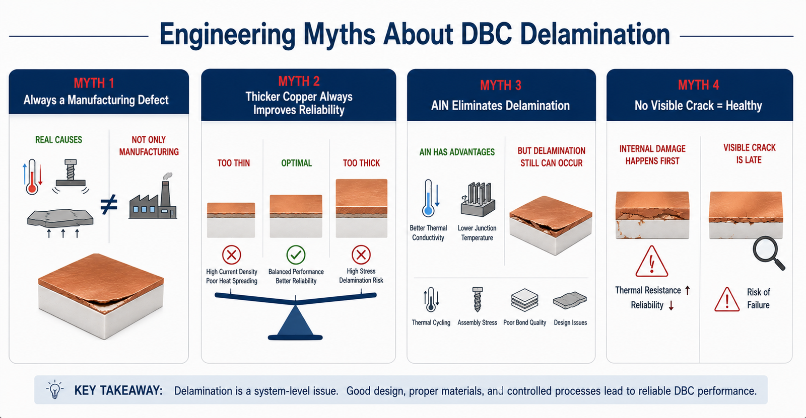
Engineering Myths About DBC Delamination
In engineering practice, many understandings regarding DBC layering are not entirely accurate. Several common misconceptions often lead to a deviation in design direction and can even compromise product reliability.
Myth 1: Delamination Is Always a Manufacturing Defect
Not necessarily.
Manufacturing quality certainly influences interface strength, but many delamination cases originate from application conditions rather than production defects.
Repeated thermal cycling, excessive assembly stress, poor heat sink flatness, solder fatigue, and improper module design can all generate interface stresses that gradually exceed the bond strength.
Successful reliability engineering therefore requires evaluating the complete system instead of focusing solely on manufacturing quality.
Myth 2: Thicker Copper Always Improves Reliability
Higher copper thickness increases current carrying capacity and improves heat spreading, but it also produces greater thermal expansion forces.
As copper becomes thicker, residual stress and cyclic fatigue loading may also increase.
Engineering optimization should balance electrical performance, thermal management, mechanical reliability, and manufacturability rather than maximizing one parameter.
Myth 3: AlN Completely Eliminates Delamination
Aluminum nitride provides higher thermal conductivity than alumina, helping reduce junction temperatures.
However, delamination is controlled by multiple factors including interface quality, thermal expansion mismatch, structural design, copper thickness, and operating conditions.
Selecting AlN alone cannot guarantee superior reliability.
Myth 4: If No Crack Is Visible, the DBC Is Healthy
Many interface failures begin internally long before visible cracks appear.
Thermal resistance often increases first, while electrical performance remains unchanged.
Early non-destructive inspection and reliability testing are therefore essential for identifying hidden damage.
DBC ceramic substrates remain one of the most reliable packaging solutions for modern power electronics. However, long-term reliability depends on far more than simply selecting a high-quality ceramic material.
Most delamination failures result from the combined effects of thermal expansion mismatch, residual stress, copper bonding quality, structural design, manufacturing consistency, and application conditions.
Rather than treating delamination as an isolated manufacturing issue, engineers should evaluate the complete system—including materials, bonding processes, module layout, thermal management, mechanical loading, and qualification testing.
In many successful projects, improvements in interface design and stress management contribute more to long-term reliability than simply upgrading to a more expensive ceramic material.
For manufacturers and OEM designers, understanding the mechanisms behind DBC delamination is the first step toward developing more reliable power modules with longer service life and lower maintenance costs.
Frequently Asked Questions
1. What is the most common cause of DBC substrate delamination?
Thermal cycling is generally considered the primary driving factor behind DBC delamination. Repeated heating and cooling generate cyclic stresses because copper and ceramic expand at different rates. Over time, microscopic interface cracks gradually propagate until partial or complete separation occurs. Manufacturing quality, module design, and assembly conditions also influence the final reliability.
2. Does thicker copper always increase DBC reliability?
No. While thicker copper improves current carrying capability and heat spreading, it also increases thermal stress during temperature cycling. Engineers should determine copper thickness according to electrical, thermal, and mechanical requirements instead of assuming that thicker copper automatically provides better reliability.
3. Which ceramic material offers the best resistance to delamination?
There is no universal answer. Silicon nitride generally demonstrates excellent thermal cycling durability, aluminum nitride provides superior thermal conductivity, and alumina offers an economical balance of performance and cost. The most suitable material depends on the application’s operating conditions and reliability targets rather than one material property alone.
4. Can DBC delamination be repaired?
In most cases, interface delamination cannot be permanently repaired. Once the copper–ceramic bond has separated, restoring the original bond strength is extremely difficult. For safety-critical power electronics, replacing the damaged substrate is generally considered the most reliable solution.
5. How is DBC delamination detected?
Common inspection techniques include Scanning Acoustic Microscopy (SAM), cross-sectional metallography, X-ray inspection, thermal resistance monitoring, and reliability testing. Different methods provide complementary information, allowing engineers to identify hidden interface defects before catastrophic failure occurs.
6. Why does delamination usually begin near substrate edges?
Edges and corners often experience higher stress concentrations during thermal expansion and contraction. Differences in material deformation, combined with geometric discontinuities, make these locations more susceptible to fatigue crack initiation over long-term service.
7. Does soldering influence DBC reliability?
Yes. Solder material, solder thickness, reflow profile, and residual stress generated during assembly all affect overall module reliability. Poor solder joint design may increase interface stress and accelerate delamination under thermal cycling.
8. How many thermal cycles can a DBC substrate withstand?
There is no fixed number applicable to every product. Thermal cycling life depends on ceramic material, copper thickness, module design, operating temperature range, heating rate, cooling rate, manufacturing quality, and testing conditions. Reliability should always be verified under representative service conditions rather than relying on generic cycle numbers.
9. How can engineers reduce the risk of delamination?
Reducing delamination requires a system-level approach. Engineers should optimize ceramic material selection, copper geometry, interface quality, thermal management, mechanical loading, solder design, and assembly consistency while validating performance through thermal cycling and reliability testing.
10. What should OEM buyers evaluate when sourcing DBC substrates?
OEM buyers should evaluate much more than material specifications. Manufacturing capability, interface consistency, process control, quality inspection methods, thermal cycling qualification, traceability, and long-term production stability all influence substrate reliability and should be considered during supplier selection.