
Introduction
For DBC and AMB substrates, the ceramic layer itself is often treated as a “basic material.” In reality, however, the manufacturing process behind a bare ceramic substrate is far more complex than many people expect.
Even when the same material system is used, differences in forming, sintering, flattening, or inspection standards can still lead to noticeable variations in thermal performance, flatness, and long-term reliability.
In actual production, problems rarely come from only one process step. Warpage, microcracks, dimensional instability, or poor metallization bonding are usually the result of multiple small process deviations accumulating throughout production.
This article focuses on the manufacturing flow of bare Al₂O₃, AlN, and Si₃N₄ substrates, along with several process details that are often overlooked during material selection.
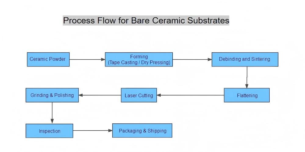
Ceramic Powder
For ceramic substrates, the quality of the powder often determines the upper limit of the final product.
Even with the same production equipment, low-grade powder can still lead to excessive porosity, unstable shrinkage, or insufficient thermal conductivity after sintering.
Al₂O₃ powder technology is relatively mature, and the industry supply chain is stable. For standard insulating substrates, 96% alumina is commonly used. However, when higher thermal conductivity or dielectric stability is required, manufacturers usually move toward 99% or higher purity grades.
AlN is far more sensitive to powder quality. Oxygen content is one of the most critical indicators because excessive oxygen directly reduces thermal conductivity after sintering. In practice, powders with oxygen levels below 1.0% are generally preferred for high thermal conductivity substrates.
Si₃N₄ behaves differently from both Al₂O₃ and AlN. During preparation, sintering additives are necessary, and the α-to-β phase transformation must be carefully controlled. If the α-phase content is too low, densification becomes difficult during later sintering stages.
For information on material selection, please read Al2O3 vs AlN vs Si3N4: which is best for power modules?
Forming Methods: Tape Casting vs Dry Pressing
Common methods for forming bare ceramic substrates include tape casting and dry pressing.
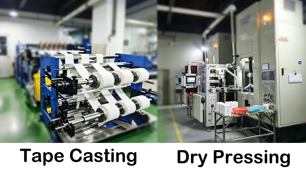
Tape casting
Ceramic powder is mixed to form a slurry, which is then scraped into thin sheets and dried to obtain a green body. This process allows for ultra-thin forming, with a minimum thickness of 0.1 mm and a thickness tolerance controlled within ±0.05 mm.
Power module substrates, especially those requiring subsequent DBC (Direct Bonded Copper) or AMB (Active Metal Brazing) processes, are almost exclusively produced using tape casting.
Dry Pressing
Dry pressing involves directly pressing powder. While the mold cost is high, the cost per unit is low. It has significant limitations: it’s difficult to produce products with a thickness less than 1 mm, and the thickness tolerance is relatively large. Therefore, this process is typically suitable for manufacturing thick-film substrates, gaskets, etc., but is rarely used for power module substrates.
| Comparison Item | Tape casting | Dry Pressing |
| Minimum Thickness | 0.1 mm | ≥ 1.0 mm |
| Thickness Tolerance | ± 0.05 mm | ± 0.1 ~ 0.2 mm |
| Surface Flatness | Excellent | Average |
| Applications | Power module substrates | Thick-film, structural components |
Debinding and Sintering: More Sensitive Than It Appears
After forming, the green body still contains a considerable amount of organic material, including binders, dispersants, and plasticizers. These substances must be removed before densification begins.
Although debinding and sintering are often discussed separately, in mass production they are usually completed continuously inside the same furnace system.
For ceramic substrates, the debinding stage is often more sensitive than many newcomers expect. If the heating rate is too fast, internal gas cannot escape smoothly, which may later cause bloating, internal pores, or even cracking after sintering.
Different materials also react very differently to furnace atmosphere control.
| Material | Sensitive Areas for Adhesive Removal | Sintering Temperature | Atmosphere Requirements |
| Al₂O₃ | 200 ~ 450℃ | 1500 ~ 1650℃ | Air |
| AlN | 250 ~ 500℃ (Sensitive to oxygen/carbon pollution) | 1700 ~ 1900℃ | Nitrogen |
| Si₃N₄ | 300 ~ 550℃ | 1750 ~ 1900℃ | Nitrogen + fueling agent |
Al₂O₃ is relatively tolerant because it is sintered in air. AlN, however, is much more sensitive to oxygen contamination and residual carbon. Once contamination occurs during debinding, thermal conductivity may drop significantly even if the substrate still appears visually normal.
In some severe cases, improperly controlled debinding can reduce the thermal conductivity of AlN substrates by 30%–50%.
Another issue that is often underestimated is shrinkage control. Actual shrinkage is not determined only by material type. Powder batch variation, green density, furnace loading, and even slight temperature fluctuations inside the furnace can all affect final dimensions.
This is why dimensional compensation is usually calculated long before mass production begins.
Flattening: Often Overlooked, Yet Extremely Important
After sintering, ceramic substrates rarely remain perfectly flat. Minor warpage is almost unavoidable, especially for large-size or thin substrates.
At this stage, flattening becomes necessary not only for appearance, but also for downstream processing stability.
A substrate with poor flatness can create multiple problems later:
- unstable laser cutting focus,
- uneven metallization,
- poor copper bonding,
- or stress concentration during module assembly.
For AlN and Si₃N₄ substrates, warpage control is generally more difficult because these materials experience larger shrinkage during sintering.
In practice, flattening quality often has a direct impact on final yield consistency.
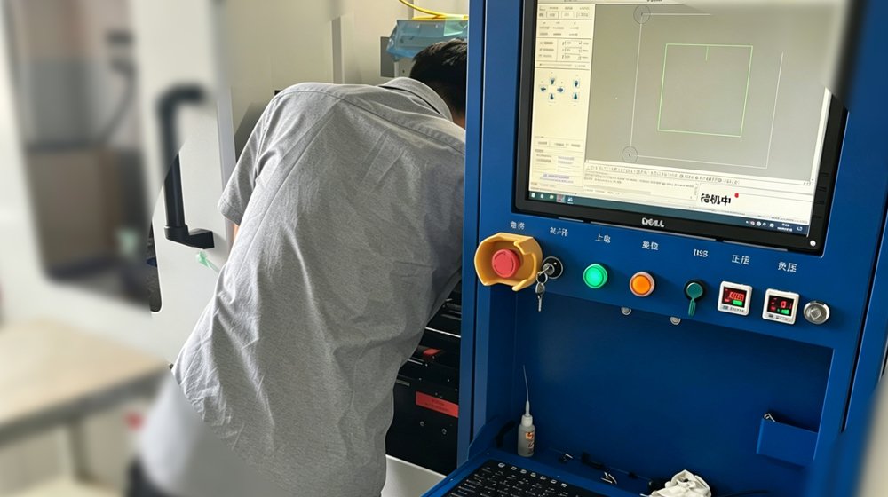
Laser Cutting
After flattening, large ceramic panels are separated into smaller substrate pieces according to the final design layout.
Compared with conventional blade dicing, laser cutting introduces far less mechanical stress, making it more suitable for brittle ceramic materials.
However, laser cutting is not simply a matter of “cutting the substrate apart.” Parameter control strongly affects edge quality and long-term reliability.
If the laser energy is too high, the heat-affected zone may enlarge and create localized damage near the cut edge. On AlN substrates, abnormal yellowing near the cutting area is often a sign that parameters are not properly optimized.
For higher-end substrates, picosecond or femtosecond lasers are sometimes used to minimize thermal influence and reduce edge microcracking.
Grinding and Polishing
The surface roughness of cut ceramic substrates typically ranges from 0.5 to 1.0 µm.
High-end substrates require grinding and polishing to control the surface roughness (Ra) within 0.1 to 0.3 µm, thereby significantly improving metallization bond strength and long-term reliability.
It is important to note that insufficient grinding can result in poor adhesion of the copper layer, while excessive grinding can cause surface damage, reduced strength, and an increase in microcracks.
Therefore, a smoother surface is not always better; a balance must be found between performance and substrate properties.
Inspection Standards for Ceramic Substrates
Inspection serves as the final checkpoint before shipment, designed to prevent defective products from entering subsequent processes.
Before shipping bare substrates, we primarily monitor the following six criteria:
1. Dimensions: Length and width must be strictly controlled within tolerance limits. Deviations will directly impact subsequent surface mount processes, making this the most fundamental requirement.
2. Thickness: Not only must tolerance requirements be met, but thickness consistency must also be ensured—uniformity directly affects thermal conductivity. If thickness is uneven, it may also result in poor bonding during module assembly.
3. Flatness/Warpage: Substrate unevenness interferes with metallization and SMT processes; products with severe warpage are immediately deemed scrap.
4. Appearance: The surface must be free of obvious defects such as pores, scratches, or foreign objects.
5. Edge Chipping: Minor edge chipping may be accepted at the customer’s discretion, but severe chipping weakens the substrate’s strength and reliability. This requires particularly strict control for substrates used in modules that must undergo vibration and thermal cycling tests.
6. Cracks: This is the most critical defect; even microscopic cracks can gradually propagate during thermal cycling, ultimately causing the substrate to fracture.
Conclusion
Bare ceramic substrates are sometimes viewed as standardized materials, but actual production tells a different story.
In many cases, the difference between a stable substrate and a failure-prone substrate does not come only from the material itself, but from how consistently the manufacturing process is controlled.
For power electronics applications, process details such as debinding stability, sintering uniformity, flattening accuracy, and crack inspection often influence long-term reliability more than expected.
As power density and thermal cycling requirements continue to increase, bare ceramic substrate manufacturing is gradually becoming less of a simple material issue and more of a process integration challenge.
FAQ
Q1: When is an Al2O3 substrate suitable, and when is an upgrade necessary?
A1: When power density is low and operating conditions are not demanding, an Al2O3 substrate is sufficient.
If power increases and heat dissipation pressure rises, an AlN substrate must be used.
For automotive-grade applications requiring frequent thermal shocks or a 15-year lifespan, a Si3N4 substrate should be used.
Q2: How to choose the thickness of a ceramic substrate?
A2: It mainly depends on voltage and heat dissipation requirements: the higher the voltage, the thicker the substrate needs to be; the higher the heat dissipation requirements, the thinner the substrate needs to be. There is a certain contradiction between the two.
0.32mm is a commonly used compromise thickness in power modules, and most modules are tested starting from this.
If the voltage is particularly high or the heat dissipation requirements are extremely tight, the thickness can be adjusted upwards or downwards according to the actual situation.
Q3: What causes warpage in ceramic substrates?
A3: The main causes are uneven sintering shrinkage or inadequate flattening processes. AlN and Si3N4 have larger shrinkage rates, making warpage more difficult to control.
Power modules typically require a warpage of ≤ 0.1%. Exceeding this range leads to uneven metallization layers and reduces chip mounting yield.
Q4: How to assess the technical level of a ceramic substrate manufacturer?
A4: It can be examined from the following key dimensions:
- Powder source (for AlN substrates, oxygen content is a key indicator).
- Temperature control accuracy and stability of the sintering furnace (the consistency in batch production should be examined).
- Quality inspection standards (the stringency of standards varies significantly among different manufacturers).
- The most direct verification method is to request CPK data from multiple consecutive batches of products. Manufacturers with minimal data fluctuations demonstrate true production stability. Using only high-quality data from a single batch as a reference cannot fully reflect their overall level.