


Introduction
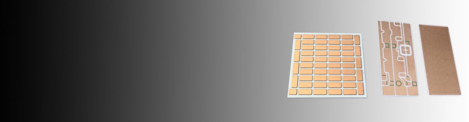
DBC (Direct Bonded Copper) ceramic substrate is an advanced metallized ceramic substrate technology that directly bonds copper layers onto ceramic materials through a high-temperature bonding process.
The structure consists of a ceramic insulating layer sandwiched between copper layers on both sides. The copper surface can be patterned through etching processes to form electrical circuits, similar to traditional PCB structures.
Compared with conventional PCB materials, DBC substrates provide superior thermal conductivity, electrical insulation, mechanical stability, and high-temperature reliability, making them widely used in demanding power electronic applications.
*DBC is sometimes referred to as DCB (Direct Copper Bonded) in some technical documents, although DBC is the more commonly accepted industry abbreviation.
DBC Ceramic Substrate Structure and Material
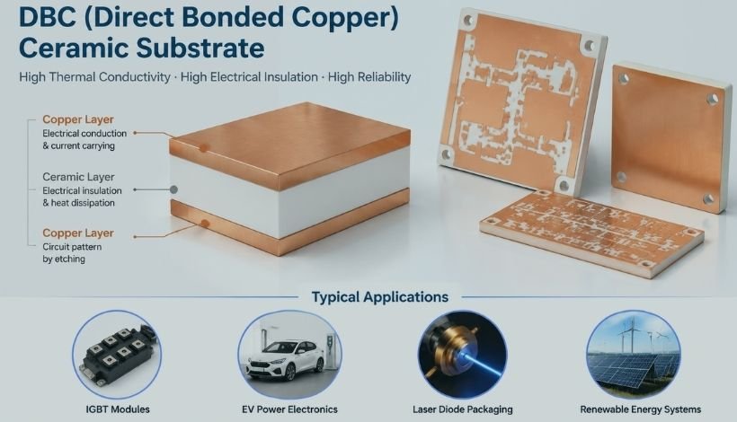
A typical DCB substrate consists of:
Copper Layer: Provides electrical conduction and current carrying capability.
Ceramic Insulating Layer: Provides electrical insulation while transferring heat efficiently.
Copper Circuit Layer: Can be etched into customized circuit patterns.
Material Options:
Alumina Ceramic DCB Substrate (Al₂O₃)
Alumina is the most commonly used DCB ceramic material due to its balanced thermal performance, electrical insulation, mechanical strength, and cost efficiency.
Typical applications include:
- IGBT modules
- Industrial power electronics
- Motor controllers
- General semiconductor packaging
Aluminum Nitride DCB Substrate (AlN)
Aluminum nitride provides significantly higher thermal conductivity compared with alumina, making it suitable for applications requiring efficient heat dissipation.
Typical applications include:
- High-power semiconductor modules
- EV power systems
- Laser devices
- Advanced thermal management systems
Our Typical Products for DBC Ceramic Substrates
Different applications have varying requirements for the performance, structure, and precision of ceramic substrates. We can customize them according to your needs to suit the actual operating environment.
-
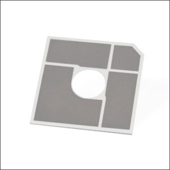
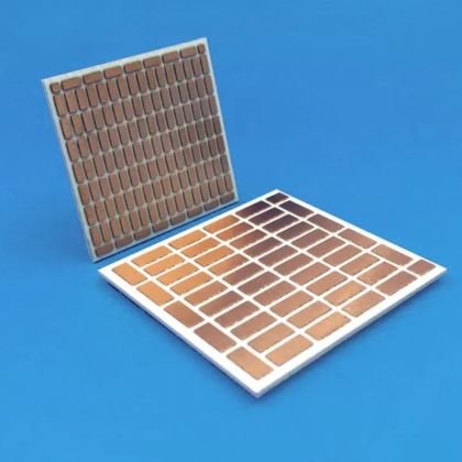 Alumina Ceramic DBC Substrates
 -
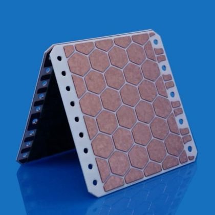 Alumina DBC Substrate for Power Electronics
 -
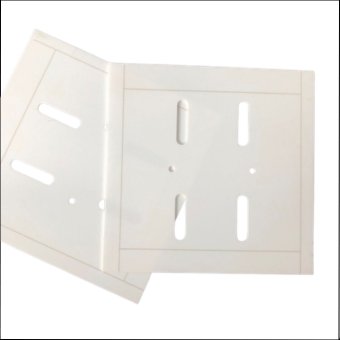
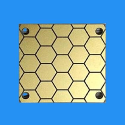 DBC AlN Ceramic Substrate
 -
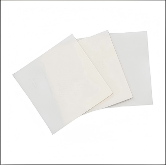
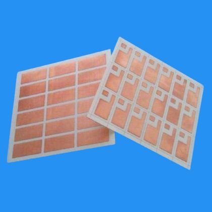 DBC Ceramic Substrates for Electronics
 -
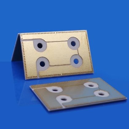 DBC Substrate With Gold Plating
Key Advantages of DBC Substrates
DBC reliability =thermal design + material matching + stress control. Most failures are caused by thermal stress rather than material defects.

The ceramic layer provides efficient heat transfer while maintaining electrical insulation, helping improve power module reliability.

DCB substrates provide reliable insulation between semiconductor devices and heat dissipation structures.

The direct bonding structure provides strong adhesion between copper and ceramic layers.

The matched thermal expansion characteristics between ceramic materials and semiconductor components help reduce thermal stress during operation.
Product Packaging
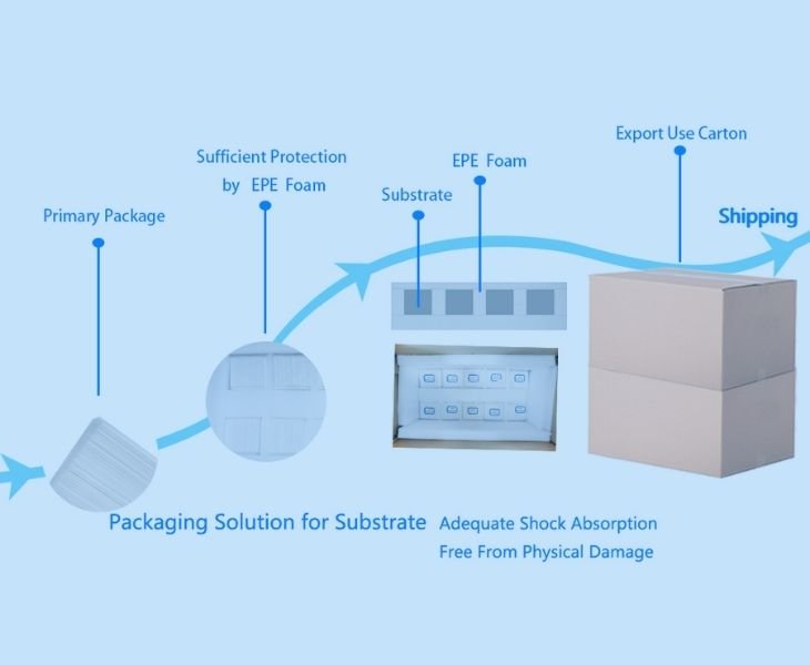
Vacuum packaging is very important for DCB direct copper bonded substrates to prevent oxidation, keep clean, prevent moisture intrusion and static electricity protection. Through vacuum packaging, the quality and reliability of the substrate can be improved to ensure that it is not damaged and affected during transportation and storage.
DBC Substrate vs PCB
Both DBC substrate and PCB are key components in electronic devices, yet they differ significantly in their applications and characteristics.
| Feature | DBC Ceramic Substrate | PCB |
|---|---|---|
| Insulation Material | Ceramic | FR4 / Resin |
| Thermal Conductivity | High | Low |
| High Temperature Performance | Excellent | Limited |
| Power Density Capability | High | Medium |
| Application | Power Electronics | General Electronics |
We provide customized DBC ceramic substrate solutions based on customer requirements. Capabilities include:
- Alumina DCB substrates
- AlN DCB substrates
- Custom dimensions
- Copper pattern design
- Prototype development
- OEM production
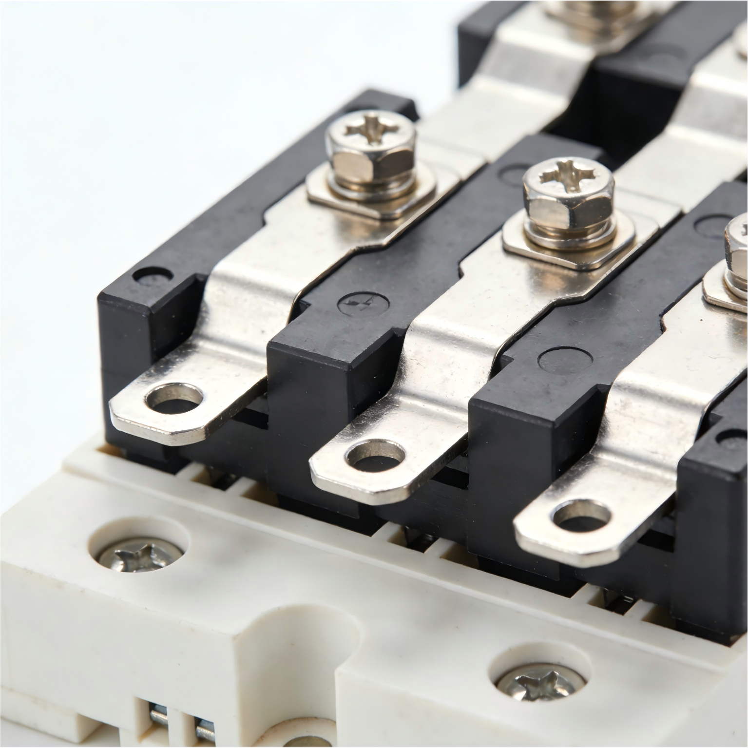
DBC substrates are mainly used in power semiconductor applications including IGBT modules, electric vehicle inverters, industrial power converters, laser devices, and renewable energy systems where efficient heat dissipation and electrical insulation are essential.
Manufacturing Capabilities
We provide customized DBC ceramic substrate solutions based on customer requirements. Capabilities include:
- Alumina DBC substrates
- AlN DBC substrates
- Custom dimensions
- Copper pattern design
- Prototype development
- OEM production
Quality Control
Key quality considerations include:
- Ceramic material inspection
- Copper bonding quality
- Surface cleanliness
- Dimensional accuracy
- Appearance inspection
Jinghui Ceramic strictly controls the eutectic temperature and oxygen content in the process of producing DBC ceramic substrates.
A DBC ceramic substrate is a metallized ceramic substrate where copper layers are directly bonded onto ceramic material. It combines electrical insulation, thermal conductivity, and mechanical stability, making it suitable for power electronics applications such as IGBT modules, EV systems, and semiconductor packaging.
The most common ceramic materials for DBC substrates are alumina (Al₂O₃) and aluminum nitride (AlN). Alumina provides a good balance between performance and cost, while aluminum nitride is preferred for applications requiring higher thermal conductivity and advanced heat dissipation.
The main difference is the insulating material. PCB usually uses resin-based materials such as FR4, while DBC uses ceramic materials that provide much higher thermal conductivity and temperature resistance. Therefore, DBC is more suitable for high-power and high-temperature electronic applications.
Yes. DBC ceramic substrates can be customized according to electrical design, ceramic material selection, dimensions, copper patterns, and application requirements. Prototype development and mass production support can be provided based on customer drawings and technical specifications.