


Laser Processing AlN Substrate Overview
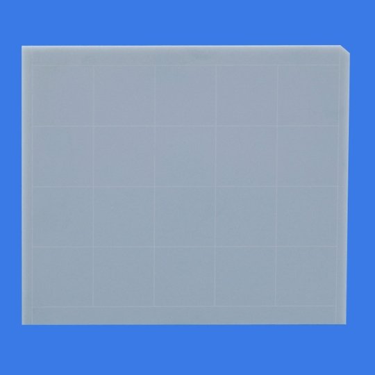
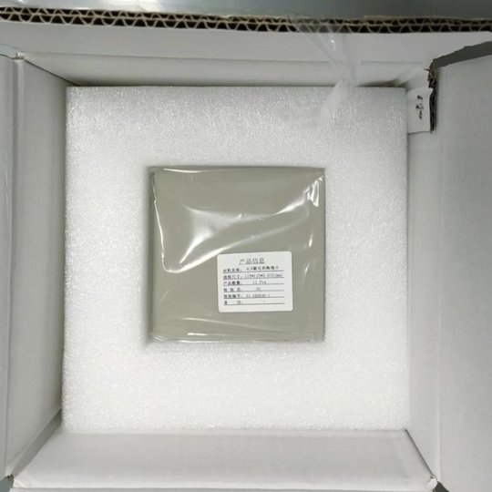
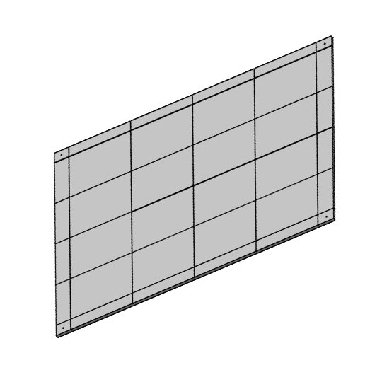
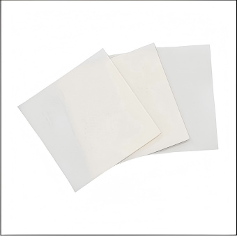
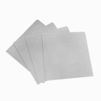
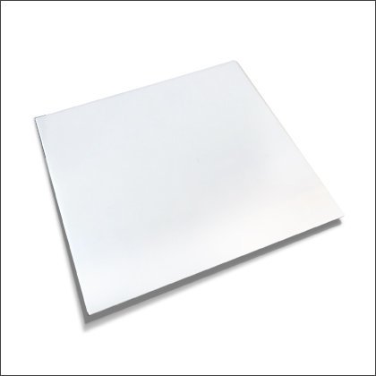
This product is a representative AlN ceramic substrate for laser cribing . It comes in standard sizes and shapes and is compatible with a wide range. Relevant dimensions are shown below.
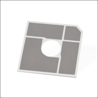
The feature of the product is as following :
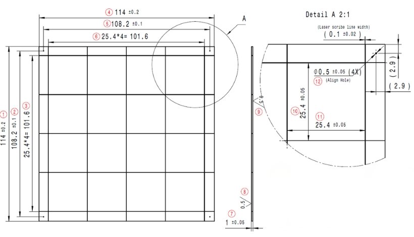
1. Ceramic substrates size:L114*W114mm, thickness and units can be different.
2. Substrate roughness: Ra< 0.5um, camber: < 0.20mm.
3. Small block size after laser scribing deepth: 45~55% of thickness.
4. Material is AlN or 96% alumina
5. Appearance requires smooth surface, no cracks, etc.
Aluminum Nitride (AlN) ceramic substrates are widely used in high-power electronic packaging due to their excellent thermal conductivity, electrical insulation, and thermal expansion compatibility with semiconductor devices.
Laser processing technology enables precise scribing, cutting, drilling, and patterning of AlN substrates while minimizing mechanical stress and edge damage. Compared with conventional machining methods, laser processing provides higher precision, better consistency, and improved efficiency for advanced ceramic applications.
Advantages of Laser Scribing for Ceramic Substrates
Laser scribing is a cost-effective and high-speed process for ceramic substrate singulation, especially for thin substrates and straight-line separation. However, precise control of laser parameters, scribing depth, and substrate stress is critical to minimize microcracks, edge chipping, and reliability issues.

Laser processing enables fine feature definition and tight dimensional tolerances suitable for advanced electronic packaging, high processing speed for mass production.

Lower processing cost compared with full laser cutting.

Non-contact laser processing minimizes cracking and chipping compared with conventional mechanical methods.

Complex patterns, micro-holes, and customized shapes can be processed efficiently.

Laser technology is ideal for thin AlN substrates that are difficult to machine mechanically.

Compatible with automated production lines.
Processing Capability
We provide customized laser processing solutions for AlN ceramic substrates, including:
- Laser scribing
- Laser cutting
- Laser drilling
- Micro pattern processing
- Prototype and mass production support
Quality Control
Strict quality control is essential for laser processed ceramic substrates. Edge quality, dimensional accuracy, and thermal damage must be carefully controlled.
Inspection methods may include:
- Optical inspection
- Dimensional measurement
- Surface defect analysis
- Strength and reliability evaluation
Why Laser Processing Is Preferred for AlN
AlN ceramics have high hardness and brittleness, making conventional machining difficult and costly. Laser processing improves efficiency while maintaining excellent edge quality and dimensional consistency.
For advanced power electronics, precise substrate processing directly affects assembly accuracy and long-term reliability.
Looking for precision laser processing solutions for AlN ceramic substrates?
Contact us for technical consultation, prototype support, and customized manufacturing solutions.
Laser processing is a non-contact method that minimizes mechanical stress during machining. This is especially important for brittle AlN ceramics because it helps reduce cracking, edge chipping, and structural damage while maintaining high dimensional accuracy.
Laser scribing creates shallow grooves for controlled substrate separation, while laser cutting completely removes material to achieve full separation. Scribing is often faster and more cost-effective for thin substrates, whereas cutting is suitable for complex contours.
Improper laser parameters may introduce thermal damage, microcracks, or edge defects. However, optimized laser processing conditions can significantly reduce the heat affected zone and maintain substrate reliability for electronic applications.
Laser processed AlN substrates are widely used in power electronics, semiconductor packaging, automotive electronics, RF devices, and aerospace systems where high thermal conductivity and precise substrate geometry are required.