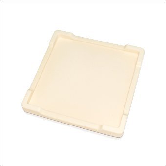

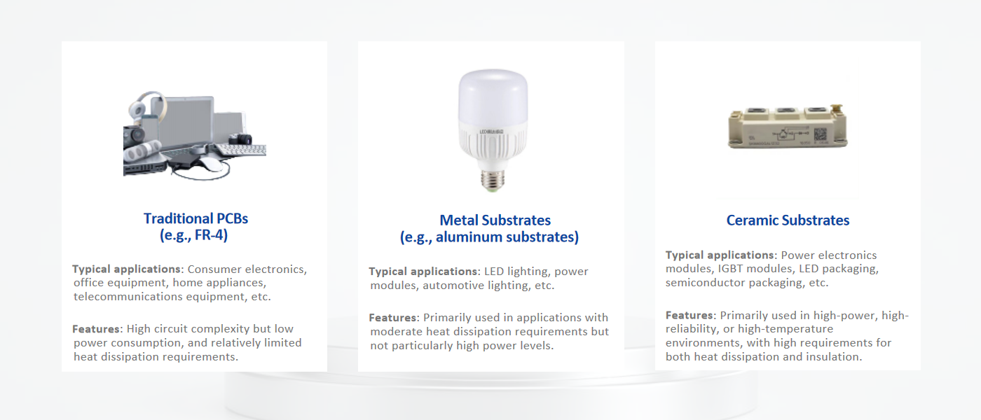
Overview of Ceramic Substrates
What Is a Ceramic Substrate
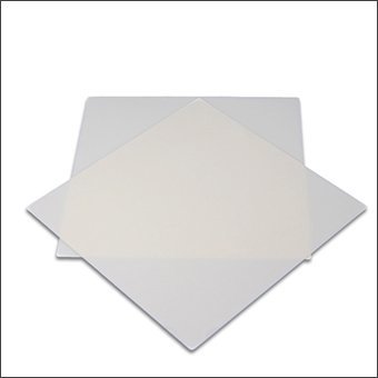
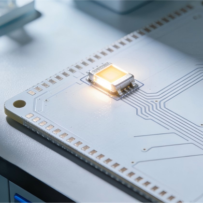
A ceramic substrate is an electronic base plate made of engineering ceramics. Its main functions are to support chips and dissipate heat quickly. It possesses both excellent thermal conductivity and electrical insulation properties, and remains stable even under high temperature or high power conditions. Compared to traditional PCBs, ceramic substrates are more suitable for electronic packaging applications with high requirements for heat dissipation and reliability.
Why Ceramic Substrates Are Used in Electronics
In electronic devices, ceramic substrates are often used as the “bottom structural component.” They not only provide mechanical support but also participate in thermal management. With increasing power density, the application of ceramic substrates is becoming increasingly widespread.
This is because the performance of traditional PCBs and metal substrates is easily limited under high-temperature or high-load environments. In contrast, ceramic substrates exhibit greater stability and are therefore gradually being adopted in some important applications.
Main Materials
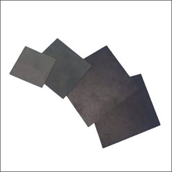
There are four commonly used materials: Alumina (Al2O3) is the most widely used material, its cost is controllable, and its manufacturing process is mature; aluminum nitride (AlN) has better thermal conductivity and is generally used in high-power applications; zirconia (ZrO2) is more focused on mechanical strength and toughness; and silicon nitride (Si3N4) demonstrates greater stability in terms of strength and thermal shock resistance.
Which material we should choose often isn’t a matter of “which one is best,” it’s about which property is more important in the application.
Manufacturer Capability
Ceramic substrates are widely used in power electronic modules, LED packaging, IGBT modules, and vacuum electronic devices. To meet the needs of different applications, ceramic substrates often require precision machining and surface treatment. We can do post-processing such as grinding, polishing, and laser scribing.
As for metallization, we mainly use Mo-Mn metallization process and surface treatments such as electroplating. For specific projects, we typically evaluate based on the drawings, focusing on confirming whether we can achieve the required structural design and critical dimensions. Only after confirming stable production can we proceed to the next stage of the cooperation process.
Types by Material
Ceramic substrates can be classified into several categories according to their materials. Different materials have significantly different properties, which will affect thermal conductivity, strength and high temperature resistance. Material selection must be based on specific applications.
Mature manufacturing process, relatively low cost, and good insulation properties.
Excellent thermal conductivity is an outstanding feature of aluminum nitride substrate.
Core competitiveness lies in the perfect combination of high strength and toughness.
High temperature and thermal shock resistance, and balanced performance.
Types by Metallization Technology
Ceramic substrates can be categorized according to metallization technology. Different metallization processes result in different metal layer structures on the ceramic surface. The three most common types are thick-film metallization, DBC (Direcet Bonded Copper), and DPC (Direct Plated Copper). Each has its own characteristics.
-
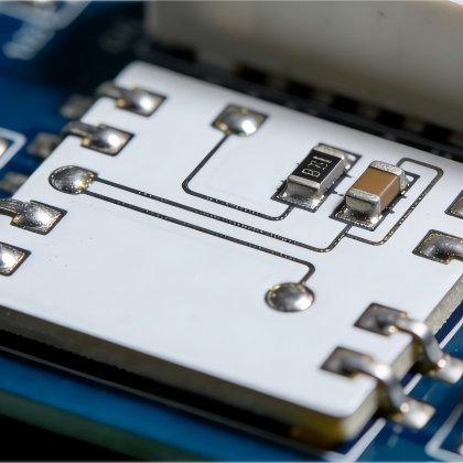
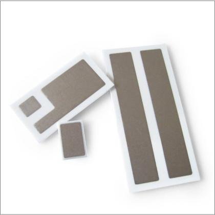 Thick Film Metallized Substrate
Printing metal paste onto a ceramic surface and sintering to form a circuit.
-
 DBC Substrate
Direct copper lamination onto ceramic, offering excellent thermal conductivity and a strong bond.
-
 DPC Substrate
First form the metallization layer, then electroplate copper, resulting in a strong bond and high reliability.
Types by Application
Ceramic substrates can be categorized by application area. Major applications are in power electronics, IGBTs, LEDs, and semiconductor packaging. Each application has specific requirements for heat dissipation and reliability.
-
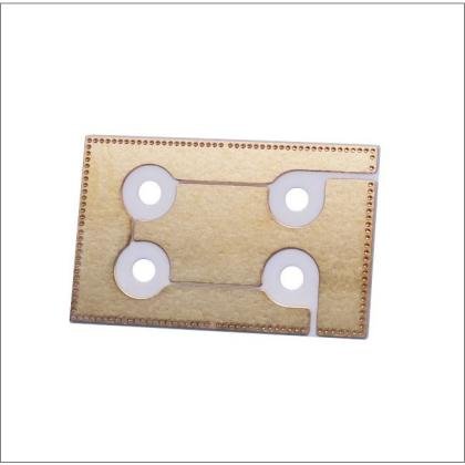
 Power Electronics Substrate
Supports power devices, with high thermal conductivity and high insulation.
-
 IGBT Module Substrate
Suitable for power switching devices, with excellent high-temperature stability.
-
 LED Module Substrate
Strong heat dissipation performance, ensuring the longevity of the light source.
-
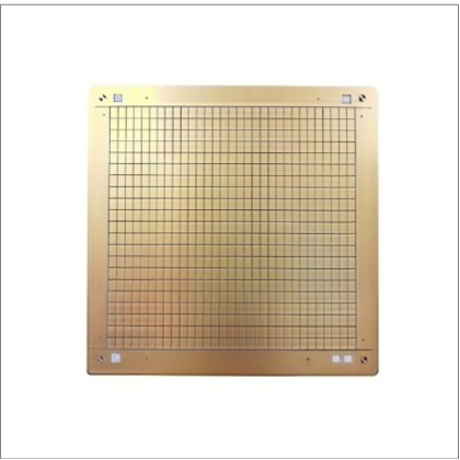
 Semiconductor Packaging Substrate
Precision dimensions, high reliability; suitable for chip packaging.
Advantages of Ceramic Substrate
The advantages of ceramic substrates primarily lie in the comprehensive performance of the material itself. Compared to traditional PCB substrates such as FR-4 or aluminum-based copper-clad laminates, they offer significant advantages in thermal management, electrical performance, and reliability.
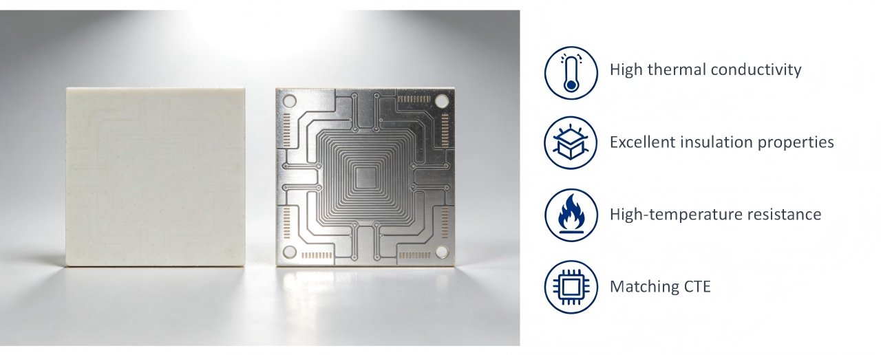
Firstly, they possess high thermal conductivity. For example, aluminum nitride substrates have high thermal conductivity, making them suitable for heat dissipation in high-power devices; while alumina substrates have lower thermal conductivity than aluminum nitride, they still meet the heat dissipation requirements of most power electronics.
Secondly, they exhibit excellent insulation properties. Ceramic materials inherently possess good electrical insulation characteristics, effectively preventing electrical interference and breakdown risks in high-voltage or high-density wiring applications.
Thirdly, they offer high-temperature resistance. Materials like zirconia and silicon nitride maintain structural stability under high-temperature environments, making them suitable for demanding operating conditions.
Another crucial point is the matching coefficient of thermal expansion. The CTE of ceramic materials is typically close to that of semiconductor chips or metal packaging materials, reducing stress accumulation during temperature cycling and thus improving overall reliability.
Applications of Ceramic Substrates
Ceramic substrates, due to their excellent thermal conductivity, insulation, and reliability, are used in many fields with high power and temperature requirements.
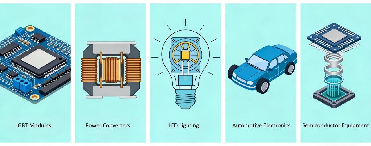
In IGBT modules, ceramic substrates are mainly used as insulation and heat dissipation support layers for power devices. Aluminum nitride and silicon nitride substrates, in particular, exhibit greater stability under high power density and high-temperature cycling environments, effectively improving module reliability.
In power converters (such as power modules and inverters), ceramic substrates are commonly used for electrical isolation and heat conduction paths for power semiconductors. They help devices dissipate heat more efficiently while ensuring electrical safety, making them suitable for medium to high-power applications.
In LED lighting, ceramic substrates are mainly used for high-power LED packaging and heat dissipation substrates. Aluminum nitride substrates, due to their good thermal conductivity, are often used in lighting products with high brightness and lifespan requirements; alumina substrates are more commonly used in conventional power LED applications.
In automotive electronics, ceramic substrates are commonly found in components such as electric drive systems, power control modules, and automotive power supplies. The automotive industry demands high levels of temperature control and reliability, making silicon nitride and aluminum nitride materials widely used.
In semiconductor equipment, ceramic substrates are used in high-precision power modules, radio frequency components, and structural parts operating in vacuum or high-temperature environments. Zirconia and silicon nitride, due to their stability and environmental resistance, are also used in some critical applications.
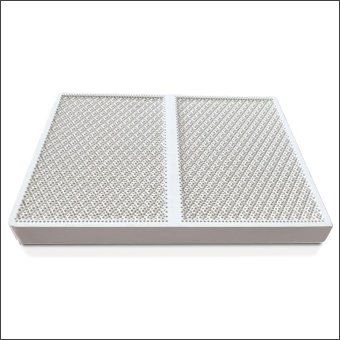
Ceramic Substrate Manufacturing Overview
The manufacturing process for ceramic substrates includes multiple steps such as forming, sintering, and machining. Different processes directly affect dimensional accuracy, surface finish, and overall reliability. We need to tailor the process based on the product’s structure and intended application.
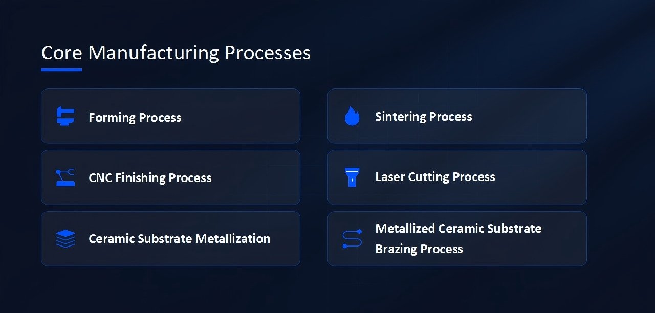
Forming Process: Includes tape casting and dry pressing. Tape casting is suitable for thin sheets with uniform thickness. Dry pressing is better suited for thicker sheets, offering better dimensional stability.
Sintering Process: The process of sintering a formed green body at high temperatures to make it dense.
CNC Finishing Process: Used to control dimensions and tolerances. It can machine structures like holes and steps. It offers high precision but is relatively more expensive.
Laser Cutting Process: Suitable for grooving and shaping. It is fast and flexible, suitable for small to medium batch production or complex structures.
Ceramic Substrate Metallization: Forming a metallization layer on the surface of the ceramic substrate. Used for subsequent brazing and conductive connections. Common metallization processes, such as the Mo-Mn process, offer high bond strength.
Metallized Ceramic Substrate Brazing Process: Used for sealing ceramics to metals. It can achieve hermetic seals. Commonly used in packaging and structural component assembly.
Why Choose Our Ceramic Substrates
When choosing our ceramic substrates, the focus isn’t just on the product itself, but also on our overall integration capabilities. From materials to processing and delivery, we strive to keep the process in-house as much as possible. This allows for easier quality control and adjustments based on customer needs. Many details require repeated verification, so responsiveness and engineering experience are equally important.
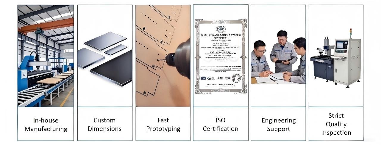
In-house Manufacturing: Major processes are completed internally. Processes are controllable. Quality is more stable, and delivery times are more predictable.
Custom Dimensions: We support customization of thickness, length, and width. We can process holes, slots, steps, and other structures. Tolerances can be controlled according to drawings.
Fast Prototyping: Short sample lead time. Facilitates customer testing and verification. Suitable for early development stages.
ISO Certification: Production and management are conducted according to established systems. Processes are standardized. Documentation and records are complete.
Engineering Support: We provide material selection and process advice. We assist in structural optimization. We reduce trial-and-error costs.
Strict Quality Inspection: Key processes are subject to testing. We control dimensions and appearance. We ensure product consistency.
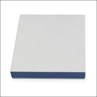
Technical Specifications Overview
The technical specifications of ceramic substrates are typically defined around material properties, dimensional ranges, and processing capabilities. These parameters vary depending on the material and processing conditions, and there is rarely a single set of data applicable to all situations.
- Our Typical Specifications
- Material Properties
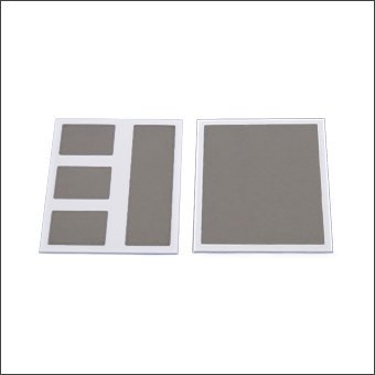
- Ceramic Substrate vs Ceramic PCB
Below are some common reference ranges, which will be helpful for initial assessments. For specific projects, we need to confirm these values based on the drawings and manufacturing processes.
| 1 | Available Materials | Al2O3 (96%, 99.6%), AlN, ZrO2, Si3N4 |
| 2 | Standard Thickness | 0.25 mm~2.0mm (depending on substrate size) |
| 3 | Maximum Size | Up to 114 × 114 mm (larger sizes may require increased thickness for process stability) |
| 4 | Surface Finish | Grinding, polishing, laser scribing, metallization |
Feel free to reach out to us to see what we can do for you.
Below are the material properties of our most common ceramic substrates for your reference. Please feel free to contact us if you have any questions about any of these parameters.
1. Mechanical Properties
| Property | Unit | 96% Al2O3 | 99.6% Al2O3 | AlN | ZrO2 | Si3N4 |
| Color | / | White | Ivory | Gray | Ivory | Black |
| Density | g/cm3 | ≥3.70 | ≥3.95 | ≥3.33 | ≥6.0 | ≥3.2 |
| Light Reflectivity | % | 70%~80% | 75%~85% | 25%~35% | 90% | 25%~40% |
| Flexural Strength | MPa | >350 | >500 | ≥380 | >800 | ≥700 |
| Fracture Toughness | MPa·m1/2 | 3.5~4.2 | 3.0~3.8 | 2.7~3.5 | 6.5~8 | 6.0~7.0 |
| Vickers Hardness | HV | 1500~1650 | 1600~1750 | 1200~1400 | 1230 | 1420 |
| Young’s Modulus | GPa | 300~350 | 370~400 | 310~350 | 200 | 290~310 |
| Camber | Length‰ | T≤0.3: ≤5‰, Others: ≤3‰ | ≤3‰ | ≤3‰ | ≤5‰ | ≤5‰ |
2. Thermal Properties
| Property | Unit | 96% Al2O3 | 99.6% Al2O3 | AlN | ZrO2 | Si3N4 |
| Max. Service Temperature (Non-loading) | ℃ | 1200 | 1400 | >1000 | 1500 | 1400 |
| CTE (Coefficient of
Thermal Expansion) @ 20-400℃ |
1×10⁻⁶/℃ | 7.0~7.5 | 6.5~7.2 | 4.2~4.8 | 9.0~11 | 3.0~3.2 |
| Thermal Conductivity @ 20℃ | W/(m·k) | 20~25 | 28~35 | 170-230 | 3 | 20 |
3. Electrical Properties
| Property | Unit | 96% Al2O3 | 99.6% Al2O3 | AlN | ZrO2 | Si3N4 |
| Dielectric Constant | / | 9.0~9.5 | 9.5~10.0 | 8.6~9.0 | 29 | 7~8 |
| Volume Resistivity | Ω·cm | >1014 | >1015 | >1014~1015 | >1013 | >1014 |
| Dielectric Strength | KV/mm | 10~15 | 15~25 | 15~25 | 9 | 13 |
While ceramic substrates and ceramic PCBs sound similar, they differ in practical applications, primarily in their functional focus and manufacturing process.
Ceramic Substrates
Ceramic substrates are more like “material base plates.” They generally refer to ceramic carriers without fully fabricated circuitry; they may have only undergone forming, sintering, grinding, or metallization (such as Mo-Mn). They are mainly used for subsequent packaging or further processing, such as as the basic structural components of power modules.
Ceramic PCBs
Ceramic PCBs are more like “boards with pre-made circuitry.” They are built on a ceramic substrate with pre-made circuitry (such as wiring, patterning, and copper plating), and can be directly used for electronic assembly or component soldering.
Ceramic substrates are mainly used to support electronic devices and provide heat dissipation, while also offering electrical insulation protection. They are commonly found in power electronic modules, LED packaging, IGBT modules, etc., improving device stability and lifespan.
Among common ceramic substrate materials, aluminum nitride has the highest thermal conductivity, significantly better than alumina. It is suitable for high-power, high-heat-flux-density applications and is more commonly used in scenarios with high heat dissipation requirements.
Alumina substrates are low-cost and have mature processing technology, making them suitable for most conventional applications; aluminum nitride substrates have better thermal conductivity but are more expensive, typically used for high-power products or products with higher heat dissipation requirements.
Yes. Common metallization methods for ceramic substrates include Mo-Mn metallization and DBC process, which are used to form a conductive layer on the surface to facilitate brazing and electrical connection, and are common steps in electronic packaging.
The thickness of ceramic substrates typically ranges from 0.25 mm to several millimeters. The specific thickness that can be produced depends on the material type and forming process, and different applications have different thickness requirements.
Ceramic substrates are mainly used in power electronics, LED lighting, IGBT modules, and semiconductor packaging industries, where high levels of heat dissipation and insulation performance are required.