

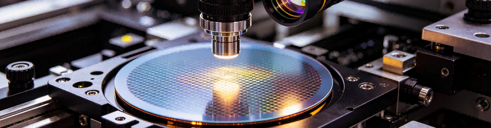
Why Technical Ceramics Solve Semiconductor Equipment Challenges
Semiconductor processes expose materials to a range of harsh operating conditions. Each of these challenges requires specific material properties to ensure stable and reliable performance. The following examples illustrate how technical ceramics address key issues in semiconductor environments:
Gradual Performance Degradation Caused by Plasma Exposure
In plasma etching environments, high-energy ions and reactive species continuously bombard material surfaces, leading to erosion, chemical reactions, and performance degradation over time. Technical ceramics such as alumina and yttrium oxide offer excellent plasma resistance due to their chemical stability and strong bonding structures. This helps reduce material erosion, extend component lifetime, and minimize particle generation.
Strict Outgassing Requirements in High Vacuum Environments
In high and ultra-high vacuum systems, even minimal outgassing can contaminate the chamber and affect process stability. Technical ceramics are inherently low in outgassing due to their dense microstructure and high purity. This makes them well-suited for vacuum applications where material cleanliness and stability are critical.
Thermal Stress and Cracking from Rapid Temperature Cycling
Semiconductor processes often involve rapid heating and cooling cycles, which can induce thermal stress and lead to cracking in less stable materials. Technical ceramics provide excellent thermal stability and resistance to thermal shock, maintaining structural integrity even under fluctuating temperatures. This ensures reliable performance in dynamic process conditions.
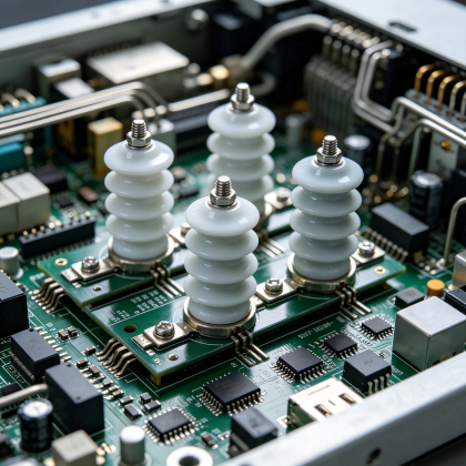
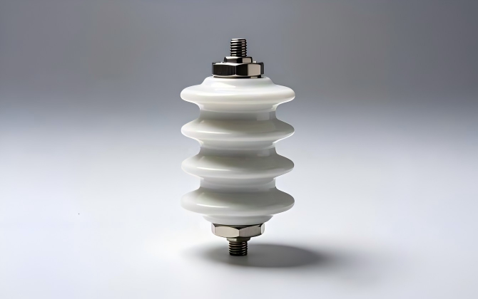
High-Voltage Insulation in Compact Systems
As semiconductor equipment becomes more compact and precise, materials must provide reliable electrical insulation within limited space. Technical ceramics offer high dielectric strength and stable electrical properties, enabling safe and consistent operation in high-voltage environments without compromising design constraints.
Particle Contamination Affecting Yield
Particle generation from material degradation is a major concern in semiconductor manufacturing, as it directly impacts yield and device performance. Technical ceramics, when properly processed and finished, exhibit high surface integrity and resistance to wear and corrosion. This helps reduce particle release and supports cleaner processing environments.
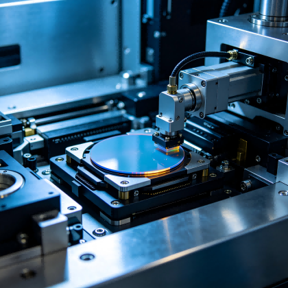
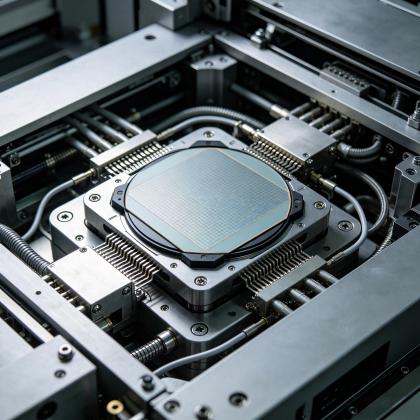
Semiconductor Equipment Applications
In semiconductor equipment, technical ceramics are widely used in many key process steps to meet the stringent requirements of high purity, high vacuum, and high reliability. With their excellent thermal stability, electrical insulation, and corrosion resistance, technical ceramics play a crucial role in improving equipment stability and process consistency.
-
High-precision ceramic arms, pins, and guides for contamination-free wafer transfer.
-
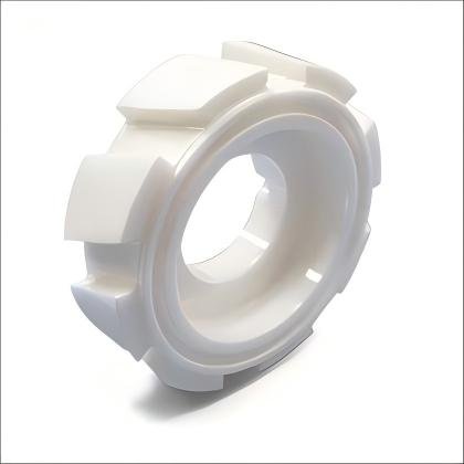
Ceramic liners, rings, and shields designed for plasma resistance and long service life.
-
Used for the transmission of electrical signals and power. Require guaranteed hermetic sealing and reliable electrical insulation.
-
High-purity ceramic insulators for electrical isolation in high-voltage systems.
-
Used for wafer adhesion and mounting. Require stable electrical properties and thermal management capabilities.
Ceramic Solutions for Semiconductor Equipment
In semiconductor devices, technical ceramics are used in several critical components. They need to withstand high vacuum, plasma, and high-reliability operating environments. These products help improve the stability and lifespan of the equipment.
-
 Metallized Ceramics for Hermetic Sealing
Reliable sealing achieved through metallization and brazing, suitable for high-vacuum and hermetic applications.
-
 Ceramic Tubes and Feedthroughs
Used for signal and power transmission in vacuum systems, combining hermeticity with electrical insulation properties.
-
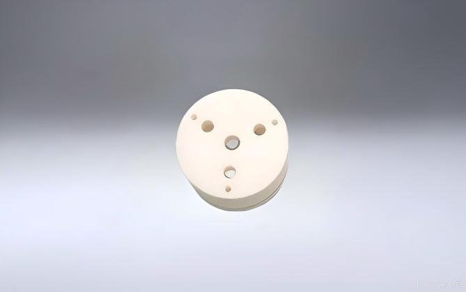
 Precision Machined Ceramic Components
Machining complex structural parts as per drawings to meet high precision, high cleanliness, and corrosion-resistant requirements.
-
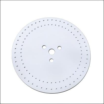 Ceramic Substrates
Good dimensional stability and electrical insulation properties. Suitable for bearing and insulating critical components in high-temperature and vacuum conditions.
Materials for Semiconductor Equipment
In semiconductor devices, different applications have significantly different requirements for material properties. The choice of technical ceramic materials directly affects the performance of components in high vacuum, plasma, and high-temperature environments. Therefore, it is necessary to select an appropriate material system based on specific operating conditions.
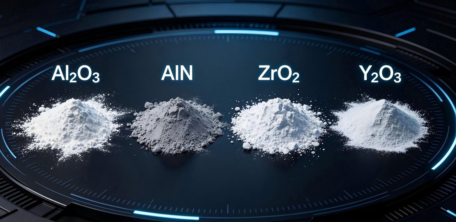
Alumina (Al₂O₃): Stable overall performance, with good electrical insulation and corrosion resistance, suitable for a variety of general-purpose components.
Aluminum Nitride (AlN): Excellent thermal conductivity and good insulation, suitable for applications with high heat dissipation requirements.
Zirconium Oxide (ZrO₂): High strength and toughness, suitable for structural components subjected to mechanical stress or impact.
Yttrium Oxide (Y₂O₃): Outstanding resistance to plasma corrosion, suitable for highly corrosive process environments such as etching.
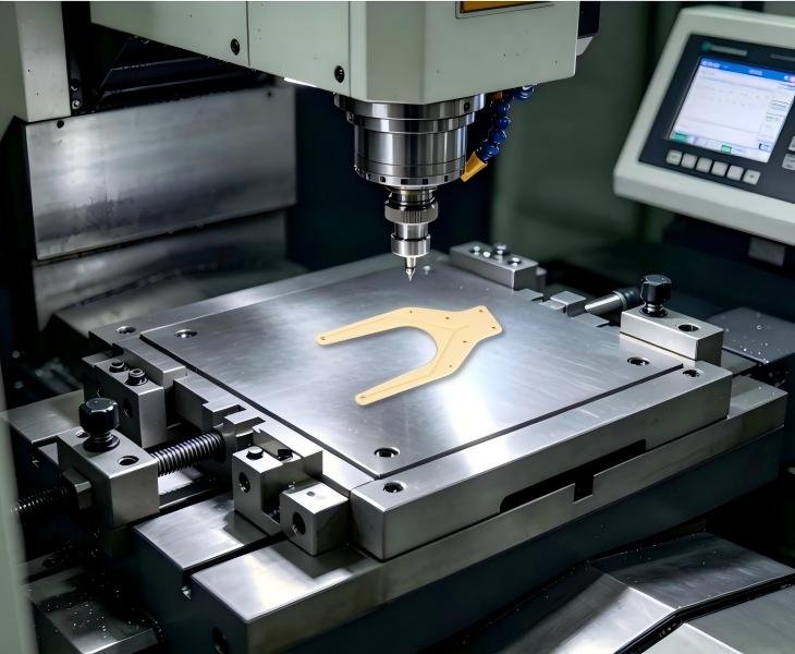
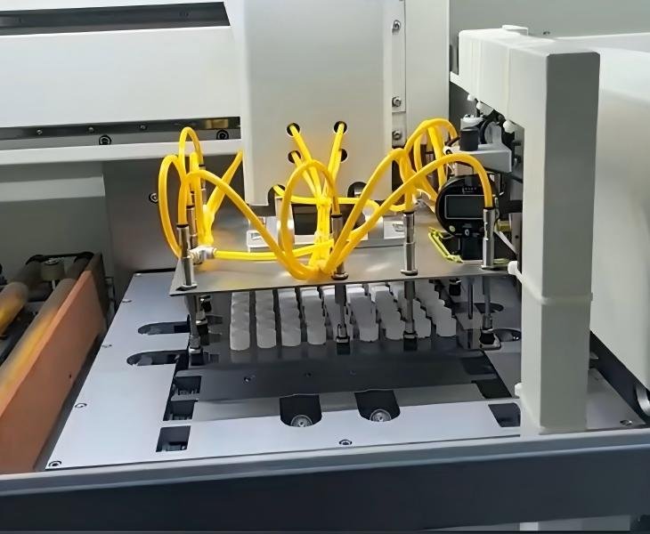
High-Precision CNC Machining Capabilities
We possess mature high-precision CNC machining capabilities for key components such as wafer handling, positioning, and support.
By combining multi-axis CNC machining with precision grinding and polishing processes, we can process ceramic parts with complex structures and high surface quality requirements. We can control critical dimensional tolerances, flatness, and surface roughness to meet the stringent requirements of semiconductor equipment for high precision and low particle count.
Furthermore, through process optimization and control, we ensure the consistency and stability of our products in mass production, making them suitable for long-term use in high-cleanliness environments.
Mature Ceramic Metallization Process Capabilities
In vacuum feedthrough and electrical connection applications, we offer mature ceramic metallization processes such as Mo-Mn metallization and DBC.
By forming a stable metallization layer on the ceramic surface, a reliable interface for subsequent brazing and electrical connections is achieved. These processes balance conductivity, adhesion, and hermeticity requirements, making them suitable for high vacuum and high pressure environments.
We can select appropriate metallization schemes based on different material systems and application needs, and through strict process control, ensure interface bonding strength and long-term reliability.
Brazing Capabilities for Hermetic Packaging
We possess comprehensive ceramic-metal brazing capabilities to meet the hermetic packaging requirements of semiconductor equipment.
By selecting appropriate solder systems and process parameters, we achieve highly reliable connections between ceramic and metal, satisfying high vacuum and hermeticity requirements. This process can be widely applied to critical components such as vacuum chamber interfaces and electrical feedthroughs.
Through optimized control of thermal stress, interface reactions, and assembly structures, we reduce the risk of cracking and leakage, ensuring stable operation of products under long-term thermal cycling and complex operating conditions.
Application Case Studies
The following are typical application cases in the semiconductor equipment field, demonstrating the actual performance and reliability of our ceramic solutions under harsh operating conditions.
- Challenge: The feedthrough module needs to operate long-term under high vacuum and temperature cycling conditions. The original structure was prone to interfacial microcracks, leading to unstable hermeticity.
- Solution: Mo-Mn metallized alumina ceramic was used, and reliable sealing was achieved through vacuum brazing. Interface and thermal stress control were also optimized.
- Results: The module achieved stable hermeticity (≤1×10⁻⁹mbar·L/s), with no significant failure after thermal cycling, improving equipment operational reliability.
- Challenge: Materials are easily corroded and generate particles in a plasma environment, affecting yield and equipment stability.
- Solution: High-purity yttrium oxide-based ceramics are used, and the microstructure and surface treatment are optimized to improve corrosion resistance.
- Results: Reduced corrosion rate, reduced particle release, extended service life, and improved process stability.
Common materials include alumina, aluminum nitride, zirconium oxide, and yttrium oxide, which are used for different applications such as insulation, heat dissipation, structural reinforcement, and resistance to plasma corrosion.
Ceramics possess excellent corrosion resistance and chemical stability, making them less susceptible to erosion or contamination in plasma environments. This helps extend component lifespan and reduce particle generation.
Yes. Ceramics have low gas release and good hermeticity, making them suitable for high vacuum and ultra-high vacuum environments. They are widely used in cavity components and feedthrough structures.
High-density ceramics, after proper processing and surface treatment, can effectively reduce particulate release, meeting the cleanliness requirements of semiconductors.
A comprehensive evaluation based on process conditions is necessary, such as temperature, plasma environment, mechanical load, and electrical performance requirements, to select the most suitable material solution.
Yes. Through metallization and brazing processes, ceramics can achieve reliable seals with metals, meeting the requirements of hermetic sealing and vacuum applications.