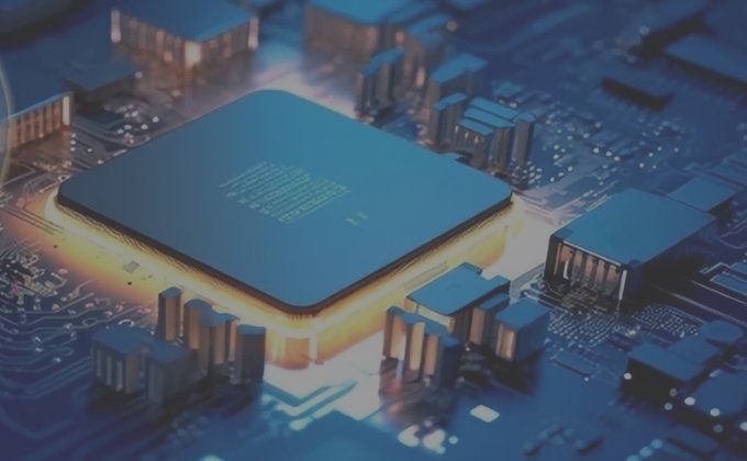

Introduction
Chips drive modern industry. However, in their nanoscale manufacturing world, extreme temperatures, strong corrosion, and high-vacuum environments pose ultimate challenges to material performance. Against this backdrop, advanced ceramics are supporting this microscopic revolution with their exceptional properties. This article will analyze the three most critical ceramic semiconductor materials: alumina, aluminum nitride, and silicon carbide.
Most Widely Used: Alumina Ceramics
Alumina ceramics were among the earliest ceramic semiconductor materials introduced. They feature high hardness, excellent insulation properties, outstanding corrosion resistance, and exceptional cost-effectiveness. These qualities have secured their enduring position in semiconductor manufacturing equipment, particularly in applications demanding abrasion and corrosion resistance.
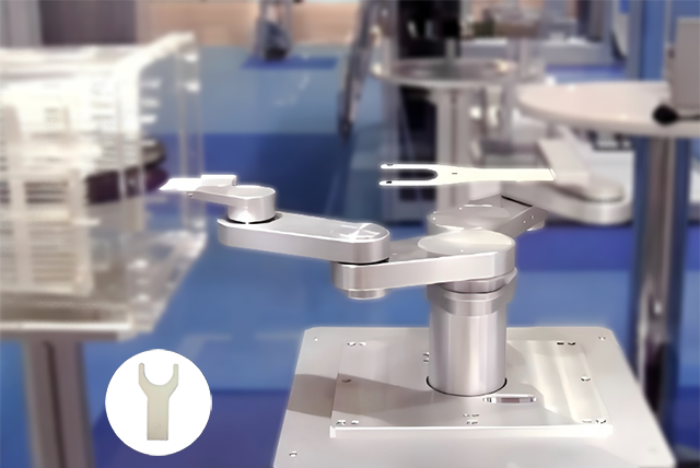
1. Wafer Transfer and Positioning Systems
End effectors and ceramic guides made of alumina ceramics play a crucial role in wafer handling in semiconductor front-end manufacturing. Alumina’s high hardness and wear resistance ensure smooth and clean wafer transport at high speeds. This effectively prevents friction-generated particles from scratching valuable wafers.
2. Plasma Etching Chamber Protection
In plasma etching, a core process in semiconductor manufacturing, insulating fixtures and guard rings made of alumina can withstand intense plasma bombardment for extended periods. This not only effectively confines the plasma zone but also protects the more valuable chamber substrate. Ultimately, this maintains a stable process environment and extends the overall life of the equipment.
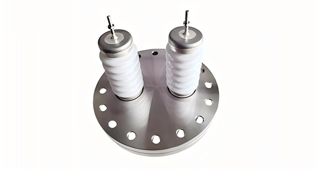
3. Vacuum Sealing and Electrical Insulation Components
In the vacuum and pressure systems required for semiconductor manufacturing, alumina ceramic feedthroughs provide both high-vacuum sealing and electrical insulation. Furthermore, thanks to alumina’s low outgassing rate and excellent corrosion resistance, the long-term cleanliness and stability of the cavity are ensured.
Preferred Heat Dissipation Expert: Aluminum Nitride Ceramics
Faced with the challenge of increasing power density in semiconductor manufacturing, efficient heat dissipation has become a core technology. Aluminum nitride ceramics, with their excellent thermal conductivity, have become a key material for solving thermal management challenges.
1. High-Power Chip Packaging Substrates
For high-power chips, aluminum nitride substrates function as “thermal highways.” They rapidly dissipate the substantial heat generated by the chip core. Aluminum nitride’s exceptional thermal conductivity directly prevents performance failures caused by chip overheating, significantly enhancing product reliability. This makes it an ideal choice for back-end semiconductor manufacturing and packaging.

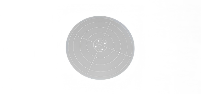
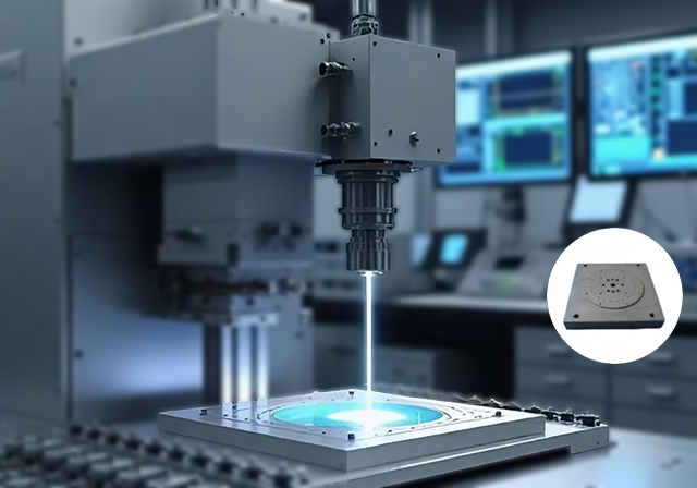
2. Vacuum Chucks
In semiconductor manufacturing processes such as wafer transport, inspection, and polishing, vacuum chucks are key components for achieving stable wafer fixation and precise positioning. Aluminum nitride ceramic, due to its excellent overall performance, has become an ideal material for manufacturing high-performance vacuum chucks.
3. Rapid-Response Ceramic Heaters
In thermal processing steps of semiconductor manufacturing, ceramic heaters using aluminum nitride substrates demonstrate the advantages of rapid heating and precise temperature control. Specifically, their excellent thermal response speed and high thermal conductivity effectively shorten process cycles, making them an indispensable key component in high-temperature processes.
Performance Champion in Extreme Conditions: Silicon Carbide Ceramics
For the most extreme environments in semiconductor manufacturing—such as high-density plasma etching and high-temperature chemical vapor deposition (CVD)—silicon carbide has demonstrated its irreplaceable dominance. Its core properties include unparalleled resistance to plasma erosion, extreme hardness and stiffness, high thermal conductivity, and high purity with low contamination.
1. High-loss Process Consumables
In etching and CVD equipment used in semiconductor manufacturing, focusing rings and gas distribution plates made of silicon carbide ceramic face direct impact from high-density plasma. This superior resistance to plasma erosion results in an extremely long service life, significantly reducing equipment maintenance frequency and becoming a key consumable for controlling overall production costs.
2. High-temperature Heat Treatment Jigs
In high-temperature diffusion and rapid thermal processing processes of semiconductor manufacturing, silicon carbide paddles and carriers withstand repeated thermal shock cycles with ease, maintaining dimensional stability and preventing contaminant precipitation. Furthermore, their exceptional high-temperature strength and corrosion resistance ensure the high purity of wafers throughout thermal processing.
3. Lithography Machine Structural Components
In lithography machines, the core equipment of semiconductor manufacturing, silicon carbide, with its extremely high dimensional stability and specific stiffness, plays a crucial role in the manufacture of core components such as reflector brackets. Therefore, it ensures that the optical path system maintains extreme nanometer-level stability and precision despite vibration and thermal disturbances.
Conclusion
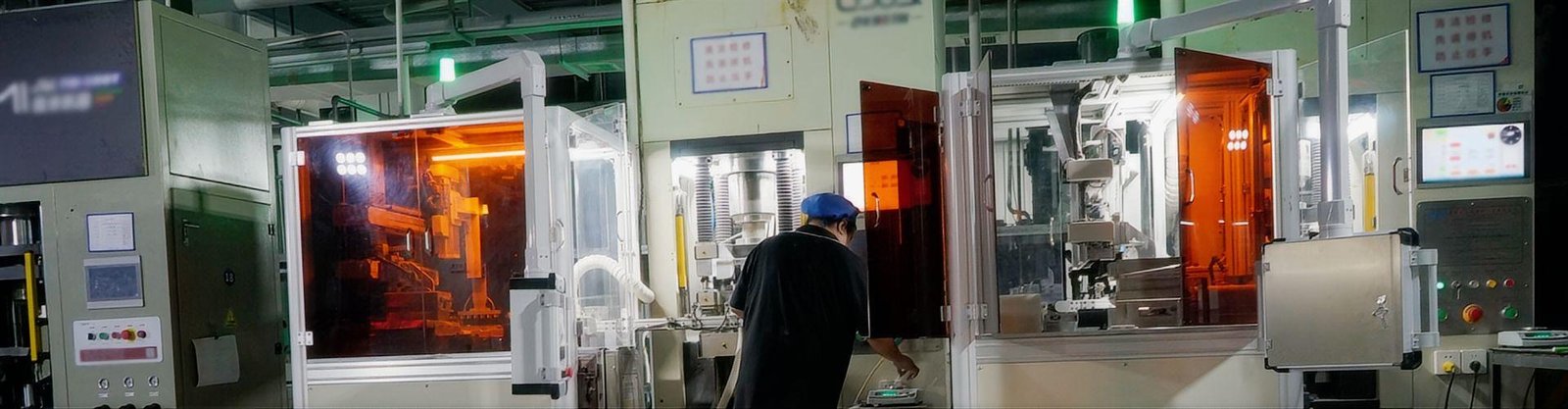
Ceramic semiconductor materials are key materials driving the continuous advancement of semiconductor manufacturing technology. Alumina (Al2O3), aluminum nitride (AlN), and silicon carbide (SiC), with their unique properties, precisely address the extreme challenges at different stages of the semiconductor manufacturing process. Together, they underpin the continuous breakthroughs in precision, power, and reliability of modern chips. As a professional supplier of advanced ceramics, we are committed to providing high-performance, high-reliability ceramic material solutions to global semiconductor equipment manufacturers.
FAQs
Q1: Why are ceramic materials widely used in semiconductor manufacturing instead of metals?
A: Ceramic materials combine high hardness, excellent electrical insulation, excellent corrosion resistance and low thermal expansion coefficient. They can simultaneously meet the extreme requirements of semiconductor manufacturing for cleanliness, vacuum integrity, insulation, and resistance to plasma erosion. This is something most metal materials cannot achieve.
Q2: What are the main differences between alumina, aluminum nitride, and silicon carbide?
A: The core difference lies in their advantageous properties:
Alumina: Excellent overall performance and the highest cost-effectiveness.
Aluminum nitride: Excellent thermal conductivity, making it the preferred choice for solving heat dissipation problems.
Silicon carbide: Highest hardness, most resistant to wear and plasma erosion, and extremely long life.
Q3: How do I choose the right ceramic material for my semiconductor device components?
A: The choice depends on the core operating conditions of the component: operating temperature, heat dissipation requirements, plasma intensity, required dielectric strength, and budget. For example, alumina is selected for transmission components, aluminum nitride is selected for heat dissipation substrates, and silicon carbide is selected for high-loss consumables.
Q4: What is the thermal conductivity of aluminum nitride ceramics? How much better is it than alumina?
A: The thermal conductivity of high-purity aluminum nitride ceramics typically ranges from 170 to 230 W/(m·K). In contrast, the thermal conductivity of alumina (99.5% purity) is approx. 30 W/(m·K). Therefore, the thermal conductivity of aluminum nitride is 6 to 8 times that of alumina.
Q5: Is it true that silicon carbide ceramics will not corrode in a plasma environment?
A: It’s not that it’s completely corrosion-resistant, but its corrosion resistance far exceeds that of other materials. In the same plasma environment, the corrosion rate of silicon carbide components is much lower than that of alumina and aluminum nitride. This means that silicon carbide has a longer service life and lower particle contamination, which can significantly reduce maintenance costs and downtime.
Q6: Can alumina ceramics be used for heat dissipation in high-power applications?
A: For low-to-medium power applications, alumina is sufficient. However, for high-power-density chips such as CPUs and GPUs, its thermal conductivity becomes a bottleneck. We strongly recommend using aluminum nitride as the thermal interface material for high-power applications to ensure chip performance and reliability.
Q7: Why choose alumina over stainless steel for wafer transfer?
A: Alumina is a hard, wear-resistant, and insulating material. It effectively prevents wafer scratches and protects chips from damage caused by electrostatic discharge (ESD). Stainless steel, on the other hand, can produce metal particles due to wear and tear, and poses an ESD risk.
Q8: Does the purity of alumina ceramics (e.g., 99.6% vs 96%) have a significant impact on performance?
A: The impact is significant. Higher purity alumina typically offers better corrosion resistance, higher electrical insulation strength, and improved thermal conductivity. For the following critical semiconductor applications, we recommend using alumina with a purity of 99.5% or higher.
1. Components directly exposed to plasma (e.g., protective rings, insulation components).
2. Vacuum chamber components requiring extremely high cleanliness and low particulate contamination.
3. Applications requiring high electrical insulation strength and high thermal conductivity.