

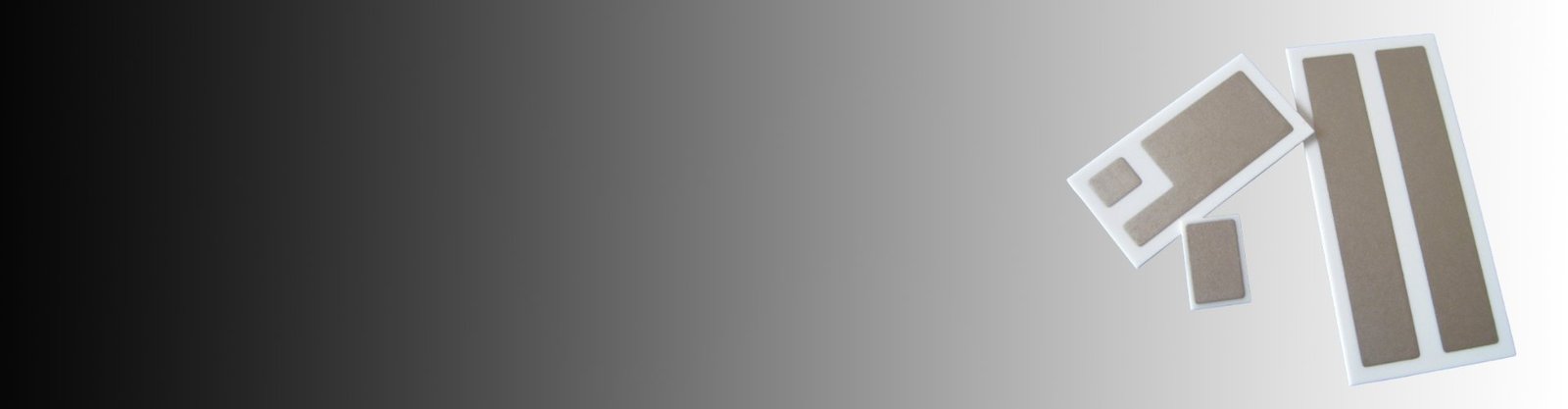
Why Metalized Ceramic Substrates
When your design faces challenges in heat dissipation, reliability or high frequency, metalized ceramic substrates are the ultimate solution. See application examples.
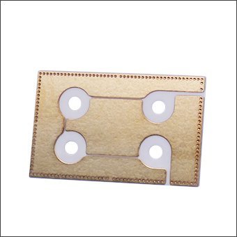
- Some home appliance control modules use thick film printed Al2O3 substrates.
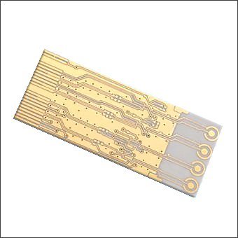
- Some industrial sensors use DBC-Al2O3 substrates.
- A fuel vehicle ECU ignition control module uses DPC-Al2O3 substrates.
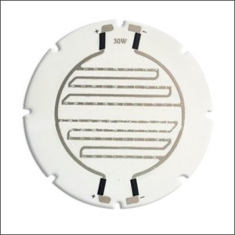
- 20W COB integrated light source uses thick film printed Al2O3 substrates.
- 5G base station AAU amplifier uses thin film AlN substrates.
- Satellite power modules use DBC-Si3N4 substrates.
High-Performance Metalized Ceramic Substrates Manufacturer
Jinghui produces high quality metalized ceramic substrates that combine ceramics (alumina or aluminum nitride) with bonded metal layers (Ni, Ag, Cu. Au, etc.).
These substrates excel in thermal management, electrical insulation, and mechanical stability, making them ideal for power electronics, LED modules, automotive systems, and RF/microwave applications.
The thickness, metallization pattern, and surface treatment can all be customized to meet the needs of different application scenarios. Our metalized ceramic substrates have strong bonding strength and the metal layer will not fall off. They have high reliability and stable performance in high temperature and high humidity environments.
By Metallization Methods
Common metallization methods for ceramic substrates include thick-film printing ceramic (TPC) metallization, thin film ceramic (TFC) metallization, direct bonded copper (DBC), direct plated copper (DPC), etc.
Thick-film printing ceramic substrate is coated with metal paste on the substrate by screen printing, and focused on Mo-Mn coating bottom layer.
Thin film ceramic substrate uses a sputtering process to deposit a metal layer directly on the surface of the ceramic substrate.
Direct bonded copper ceramic substrate utilizes oxygen element to form CuO eutectic phase, so that copper foil and ceramic eutectic bond.
First preparing through holes and sputtering metal seed layers, and then electroplating to fill the holes and thicken the metal circuit layer.
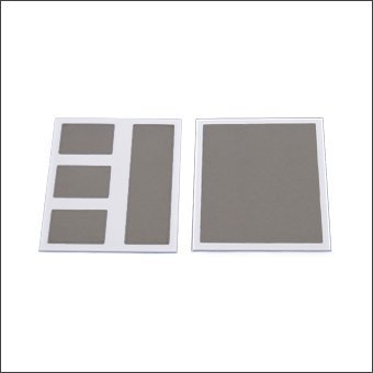
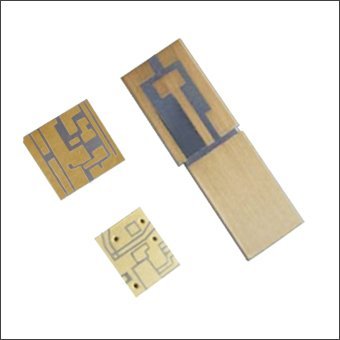
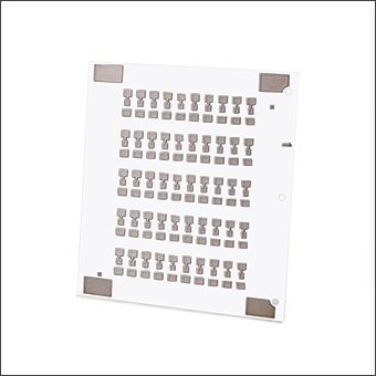
Typical Products
The Mo-Mn metallization process belongs to the thick-film printing ceramic (TPC) metallization process. It uses screen printing technology to coat the metallization slurry containing Mo and Mn on the ceramic surface, and then sintering to form a metallization layer. The Mo-Mn metalized ceramic substrate has high bonding strength, good airtightness and high reliability. It is widely used and cost-effective.
-
Molybdenum and manganese are mainly used to improve the bonding strength and air tightness between ceramics and metals.
-
Nickel plating can improve the wettability of the metallization layer and solder and enhance welding performance.
-
Silver plating improves conductivity and soldering performance and is often used in high-frequency electronic devices.
-
Gold plating improves oxidation resistance and solderability and is often used in high-reliability electronic devices.
-
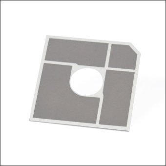
 Silver-coated 96% Alumina Substrate
No molybdenum or manganese on the bottom layer of the substrate, and silver is directly coated on the substrate.
Metalized Ceramic Substrate Vs. Traditional PCB:
In the electronics industry, metalized ceramic substrates and traditional PCBs (printed circuit boards) are two common basic materials, but they have their own advantages and disadvantages in different application scenarios.
Performance Comparison
- Thermal Conductivity
The thermal conductivity of metalized ceramic substrates (such as aluminum nitride, alumina) is much higher than that of traditional PCBs (such as FR-4), suitable for high-power applications.
- High Temperature Resistance
Ceramic substrates can work stably in high temperature environments, while traditional PCBs are prone to deformation or failure at high temperatures.
- Mechanical Strength
Ceramic substrates are more durable, but traditional PCBs are lighter and easier to process.
Application Scenarios
Metalized ceramic substrates: Suitable for high-power modules (such as IGBT, LED), automotive electronics, and aerospace, which have extremely high requirements for heat dissipation and reliability.
Traditional PCBs: More suitable for consumer electronics, communication equipment, and low-power applications because of their low cost and flexible design.
Summary
Metalized ceramic substrates have more advantages in performance and reliability, but the cost is higher; traditional PCBs occupy a place with their economy and flexibility. The choice of material depends on the specific application requirements.
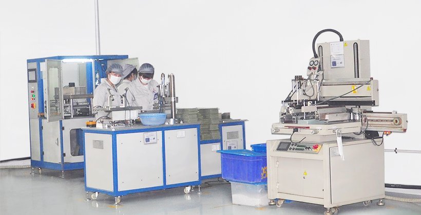
Although there are many manufacturing methods for metalized ceramic substrates (such as TPC, TFC, DBC, DPC, etc.), their core steps include: ceramic substrate preparation -> metallization layer deposition -> patterning -> surface treatment -> quality inspection.
Ceramic substrate preparation includes cleaning and surface treatment of the ceramic substrate to ensure that the surface is free of contamination, flat and suitable for metallization. The core goal of metallization layer deposition is to form a uniform, dense and highly adherent metal layer on the ceramic surface. Patterning determines the electrical properties and functions of the metalized ceramic substrate. Surface treatment enhances the adhesion between metal and ceramic, making it more durable. Finally, the finished product is strictly quality inspected.
In power electronics, metalized ceramic substrates are used in key components such as IGBT modules, power modules and inverters. Their high thermal conductivity and low thermal resistance can effectively reduce device temperature, improve system efficiency and reliability, and are particularly suitable for electric vehicles, industrial motors and renewable energy.
Common ceramic materials include alumina (Al2O3), aluminum nitride (AlN), and silicon nitride (Si3N4). Alumina has low cost and good insulation, aluminum nitride has excellent thermal conductivity, and silicon nitride has both high strength and thermal shock resistance. Choosing the right material according to application requirements can optimize substrate performance.
Metalized ceramic substrates significantly improve heat dissipation performance by combining high thermal conductivity ceramic and metal layers. Its low thermal resistance can quickly transfer heat from the heating element to the heat sink, making it suitable for high power density scenarios such as LED lighting, power modules and high-frequency communication equipment.
Thick-film printing has limited metal layer thickness and conductivity, making it unsuitable for high-power applications. It is best for low-cost and low-frequency circuits.
When selecting a supplier, pay attention to its technical capabilities, quality certifications (such as ISO9001), production experience, and customer support services. Ensure that you choose a reliable partner that meets your needs by evaluating sample performance, delivery time, and after-sales support.