

Advantages Over Traditional PCBs
Compared to traditional PCBs, metalized ceramic substrates offer the following advantages:
1. Superior electrical insulation properties
2. Excellent high-temperature and corrosion resistance
3. Higher structural strength and dimensional stability
4. Suitable for high-reliability, high-power, and high-density packaging applications
Through metallization processes, ceramic substrates can achieve welding, bonding, hermetically sealed packaging, and multilayer interconnects, making them an irreplaceable core material in advanced electronic packaging.
Experienced Metalized Ceramic Substrate Manufacturer
We are a Chinese manufacturer specializing in advanced ceramics. We can provide you with custom metalized ceramic substrates. Our vertically integrated manufacturing capability enables flexible production scaling from prototype to volume manufacturing, ensuring consistent quality and reliable delivery.
Our metallization processes are fully developed and validated, enabling stable batch production once your design is confirmed. If needed, our engineers will work with you to optimize the metallization design, layout, and material selection. Both of us will benefit from this, as it improves reliability, reduces costs, and enhances manufacturability.
Why Choose Our Metalized Ceramic Substrates
- Complete manufacturing chain from ceramic forming and sintering to metallization
- Stable batch consistency
- Strong customization capability
- Small MOQ + mass production support
Want a free technical assessment & quote support? Upload your drawings, and our engineers will respond within 24 hours.
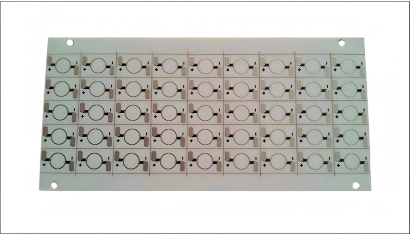
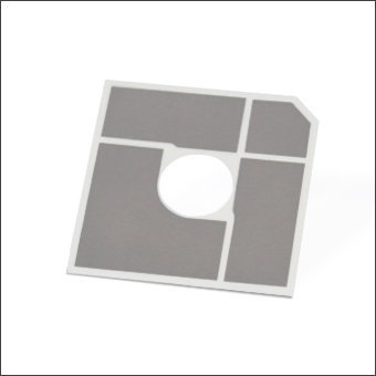
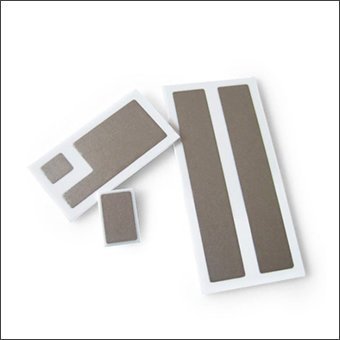
Metalized Ceramic Substrate by Metallization Process
With our extensive experience in process technology and equipment configuration, we primarily offer the following mature and stable metalized ceramic substrate solutions.
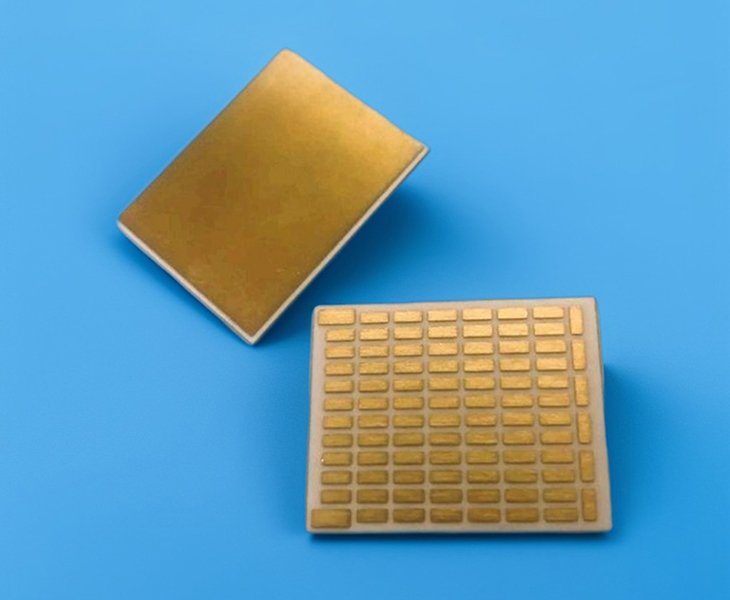
A type of hermetic ceramic package substrate. Compatible with nickel/gold plating processes. Suitable for sensor packages, vacuum devices, power modules, and medical electronics packages.
Nickel plating enhances solderability and oxidation resistance. Suitable for Au wire bonding and Sn soldering. Applied to LED packages, power modules, automotive electronic modules, etc.
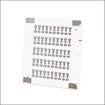
Excellent electrical conductivity and low contact resistance. Applied to high-frequency communication modules, microwave devices, precision electronic components, etc.
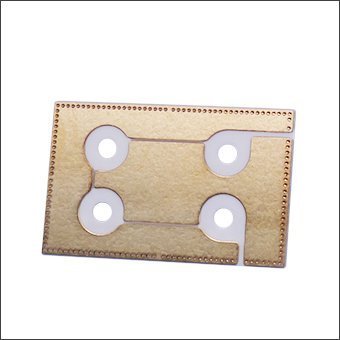
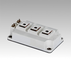
Direct bonded copper on Al2O3 / AlN. High thermal conductivity and current-carrying capacity. Applied to IGBT power modules, electric vehicle power systems, photovoltaic inverters, etc.
Ceramic Materials for Metalized Ceramic Substrates
For metalized ceramic substrates, our base materials are mainly alumina and aluminum nitride ceramics. We also do zirconia and silicon nitride but in relatively small quantities. Should you require them, we can provide small-batch customization services.
Metallized alumina substrates are the most common type we produce. Our alumina purity ranges from 94–96% to 99%.
We offer metallized aluminum nitride substrates with thermal conductivity as high as 170~190 W/(m·K).
We offer small-batch customization services for metallized zirconia substrates.
We offer small-batch customization services for metallized silicon nitride substrates.
Key Technical Parameters for Your Reference
- Minimum linewidth/spacing: ≥ 0.2 mm
- Metal layer thickness: 10–30 μm (customizable)
- Operating temperature: 300-400°C
- Metal layer adhesion strength: ≥ 15 MPa
- Hermetically sealed leakage rate: ≤ 1×10⁻⁹ Pa·m³/s
Specific parameters can be customized and optimized according to product design.
Typical Applications of Metalized Ceramic Substrates
Metallized ceramic substrates are widely used in high-end electronic packaging and power electronic systems due to their excellent insulation, thermal conductivity, and high reliability. We can provide tailored materials and metallization solutions for different application environments.
Power electronic systems place extremely high demands on the thermal conductivity, insulation properties, and thermal cycling reliability of substrate materials. Metallized ceramic substrates can effectively improve device heat dissipation efficiency and ensure the long-term stability of electrical connections.
Typical applications: IGBT power modules, SiC power devices, industrial power modules, photovoltaic inverters, and energy storage systems.
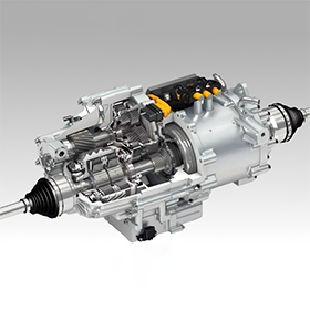
Electric vehicles place extremely high demands on the reliability of their electronic systems. Aluminum nitride and alumina metallized ceramic substrates maintain stable performance in high-temperature and vibration environments, and are therefore widely used in core electronic modules of electric vehicles.
Typical applications: electric drive control modules, on-board charging systems, battery management systems, and motor control units.
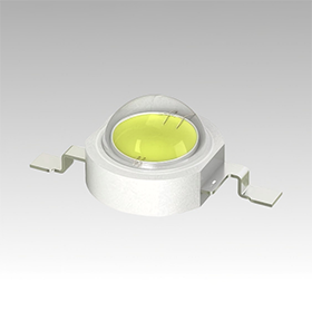
LEDs and optoelectronic devices place high demands on the thermal conductivity and soldering reliability of the substrate. Metallized ceramic substrates can effectively improve heat dissipation efficiency while ensuring the stability of electrical connections, thereby significantly extending the lifespan of the devices.
Typical applications: High-power LED packaging, UV LEDs, laser device packaging, and optical communication modules.
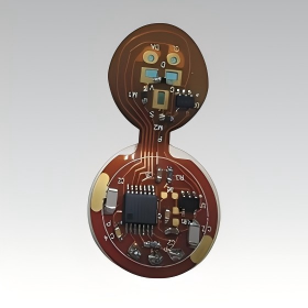
Sensor products have high requirements for hermeticity, electrical stability, and structural strength. Mo-Mn metallized ceramic substrates offer excellent hermetic sealing capabilities, effectively protecting sensitive components and enhancing the long-term stability and reliability of the product.
Typical applications: Gas sensors, pressure sensors, temperature sensors, and industrial detection sensors.
In the fields of vacuum electronics and radio frequency devices, packaging materials must possess extremely high hermeticity and thermal stability. Metallized ceramic substrates enable reliable connections between ceramic and metal structures, making them a key material for high-reliability electronic packaging.
Typical applications: Vacuum electronic devices, microwave devices, high-frequency communication modules, and aerospace electronic packaging.
Industrial automation and communication equipment demand high stability from electronic components, especially in high-frequency and complex electromagnetic environments. Ceramic substrates offer more stable electrical performance and stronger structural strength.
Typical applications: industrial automation control modules, frequency converter systems, communication base station modules, and RF power devices.
Mo-Mn metallization is a high-temperature sintering metallization process suitable for high-reliability electronic packaging and hermetic packaging.
DBC uses a direct copper foil bonding process. It offers higher thermal conductivity and current-carrying capacity. Suitable for power module applications.
Yes, we can perform metallization on aluminum nitride substrates. Please send your drawings, and we will evaluate the feasibility of production.
Yes, we can provide small-batch prototyping services for metalized ceramic substrates. Once your requirements are finalized, we can also handle large-volume production for you.
Our custom process for metalized ceramic substrates is as follows: Provide drawings / application requirements –> Engineering assessment and process suggestions –> Prototyping –> Sample delivery –> Sample validation –> Mass production –> Batch delivery.