


Preferred Electronic Ceramic Substrate Materials
With its excellent comprehensive performance, alumina substrate has become the preferred material in the electronics industry.
- Excellent electrical insulation: Suitable for supporting electronic circuits and components.
- High temperature and aging resistance: Capable of long-term operation in high-temperature and harsh environments.
- High mechanical strength and dimensional stability: Resistant to deformation, ideal for precision structures.
- Mature manufacturing processes and high cost-effectiveness: One of the most widely used ceramic substrate types.
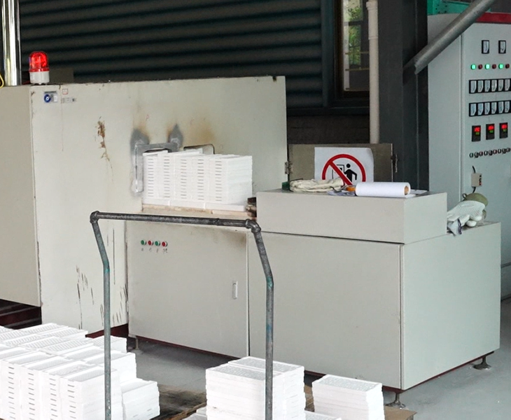
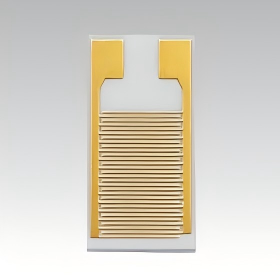
Custom Alumina Substrate Manufacturing Facility
We specialize in the production of custom alumina ceramic substrates for the electronics, power, automotive, and industrial fields. We offer long-term, stable supply. With our mature powder formulations and in-house sintering and processing capabilities, we provide highly consistent, reliable industrial-grade alumina substrate solutions.
What can we offer you?
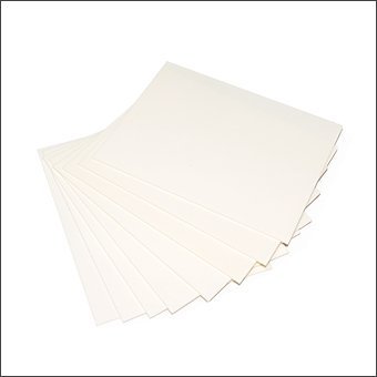
- Supports customization of 96%, 99%, and 99.6% alumina substrates.
- Covers processes such as laser cutting, CNC machining, polishing, and metallization.
- High batch consistency, suitable for long-term stable supply.
- Supports customization based on drawings or samples, with rapid prototyping.
Typical Specifications We Can Do
| Item | Our Capability |
| Material | 96% / 99% / 99.6% Al₂O₃ ceramic |
| Size Range | Max. 500 × 500 mm |
| Thickness | 0.25 ~2.0 mm |
| Flatness | ≤ 0.1% |
| Surface Roughness | Ra 0.2 ~ 0.8 μm |
| Dimensional Tolerance | ±0.15 ~ ±2 mm |
| Cutting Method | Laser / Dicing / CNC |
| Metallization | Mo-Mn, W, Ag, Ni/Au plating |
If you are looking for a reliable alumina substrate manufacturer, we can provide technical support from material selection and structural design to mass production.
Our Alumina Substrate by Material Purity
Based on material purity, alumina substrates can be classified into 96% alumina substrates, 99% alumina substrates, and high-purity alumina substrates.
Suitable for most industrial electronics and structural applications. Offers stable overall performance and high cost-effectiveness. Commonly used in power modules, control circuits, and general electronic substrates.
It possesses superior insulation performance and thermal stability. Suitable for electronic products with higher requirements for reliability and electrical performance.
Suitable for applications requiring high dielectric properties, density, and stability. Meets the needs of high-end electronics and special operating conditions.
Our Alumina Substrate by Processing Technology
Depending on the processing method, alumina substrates can be divided into laser-cut alumina substrates, CNC-machined alumina substrates, polished alumina substrates, and metalized alumina substrates.
Suitable for complex shapes and high-precision contours. High processing efficiency. Good dimensional consistency.
Suitable for ceramic substrate products with high requirements for hole positioning, slot positioning, and structural precision.
Achieves low surface roughness. Meets the requirements for thin-film circuits or precision mounting.
Supports metallization of materials such as Mo-Mn and W. Enables subsequent nickel plating or gold plating processes. Suitable for soldering and packaging applications.
Alumina Substrate Manufacturing Process
The following is a general production process for our alumina substrates. All processes are completed in-house, which helps ensure consistent quality and controllable delivery times.
- Raw material preparation and powder processing
- Forming (tape casting / dry pressing)
- Green body processing
- High-temperature sintering
- Precision machining and surface treatment
- Laser cutting or CNC machining
- Metallization and surface coating
- Full inspection and shipping
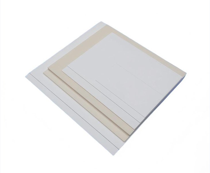
Customization Options for Our Alumina Substrates
We support the following customization options:
- Dimensions and shape
- Thickness and structural design
- Surface roughness
- Metallization areas and methods
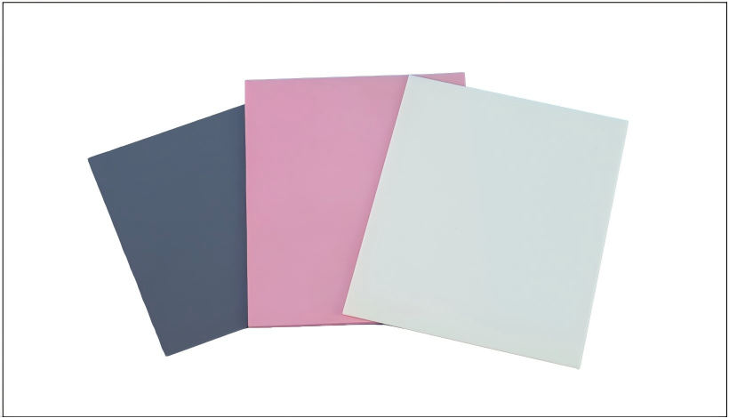
- Color options: White / Beige / Pink / Black (based on material system and application requirements)
For special requirements, please contact us in advance to discuss feasibility.
Typical Applications of Alumina Substrates
Different applications have varying requirements for the performance, structure, and precision of ceramic substrates. We can customize them according to your needs to suit the actual operating environment.
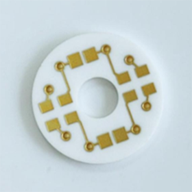
In LED applications, Al₂O₃ substrates are commonly used as the supporting structure for circuit loading and heat dissipation. They are particularly suitable for LED modules requiring electrical insulation, structural stability, and long-term reliability.
We offer alumina substrates in various thicknesses and specifications. We support metallization processing and customized contour and aperture designs tailored to specific LED structures.
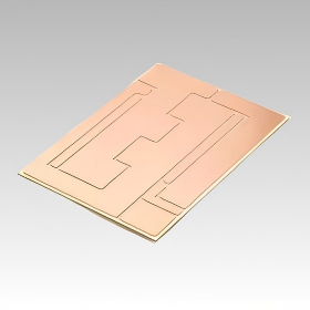
In power electronics and power supply systems, alumina substrates are used for electrical insulation and structural support of power modules. Alumina ceramics maintain good electrical performance and mechanical strength under complex operating conditions.
To meet diverse design needs, we offer custom processing services for alumina substrates of varying purities and support thick-film printing metallization on alumina substrates.
In various sensor applications such as gas sensors, pressure sensors, and temperature sensors, alumina substrates are commonly used as circuit carriers and structural base materials. Alumina materials maintain excellent performance even under high temperature, humid, or corrosive environments.
We can provide alumina substrates in various specifications and support thick-film circuit processing and customized designs.
96% alumina substrates offer a favorable balance between performance and cost, making them suitable for most industrial and electronic applications.
99% alumina substrates provide superior insulation properties, higher density, and enhanced electrical stability, making them ideal for applications demanding greater reliability.
Thick-film alumina substrates typically use 96% alumina substrates to balance performance and cost.
Thin-film alumina substrates, however, use 99% or higher purity alumina substrates to meet the TFC process requirements for surface quality and electrical property consistency.
It depends. For most industrial and power applications, thick-film alumina substrates offer a better balance between reliability and cost. Thin-film alumina substrates, however, are more suitable for scenarios demanding higher precision in circuit patterns and greater consistency in electrical performance.
The color of an alumina substrate primarily depends on material purity, added elements, and the sintering process. Common colors include white, beige, pink, and black. The color itself typically does not directly affect its insulation properties or mechanical strength.
Common thicknesses for alumina substrates range from 0.25 mm to 2.0 mm. We can customize thicknesses based on application requirements and structural design.
Certainly. Alumina substrates typically support customization across multiple aspects, including dimensions, thickness, profile structure, surface roughness, processing methods, and metallization areas.
Alumina substrates possess excellent electrical insulation properties, high-temperature resistance, and mechanical strength. They are widely used in electronic circuits, power modules, LEDs, automotive electronics, and industrial electronics.