

Boron Nitride Ceramic Material Overview
Hexagonal boron nitride (h-BN) is a non-oxide ceramic with a layered crystal structure similar to graphite, often referred to as “white graphite.”
Unlike graphite, boron nitride ceramic is electrically insulating, chemically inert to molten metals, and stable in vacuum and inert atmospheres, making it a preferred material for demanding industrial environments.
It is widely used in semiconductor manufacturing, vacuum furnaces, molten metal handling, and high-temperature electrical insulation applications, especially where graphite or alumina are not suitable.
Technical Data (Typical Values)
| Property | h-BN Ceramic | BN–SiO₂ Composite |
|---|---|---|
| Density (g/cm³) | ≥ 2.0 | ≥ 2.1 |
| Flexural Strength (MPa) | 30 – 150 | ~66 |
| Elastic Modulus (GPa) | ~30 | 40 – 74 |
| Thermal Conductivity (W/m·K) | 35 – 75* | ~25 |
| Max. Service Temperature (Air) | ≤ 900 °C | ≤ 850 °C |
| Max. Service Temperature (Inert / Vacuum) | ≤ 1800 °C | ≤ 1600 °C |
| Dielectric Strength (kV/mm) | 30 – 50 | ≥ 40 |
*Thermal conductivity depends on density, orientation, and testing direction.
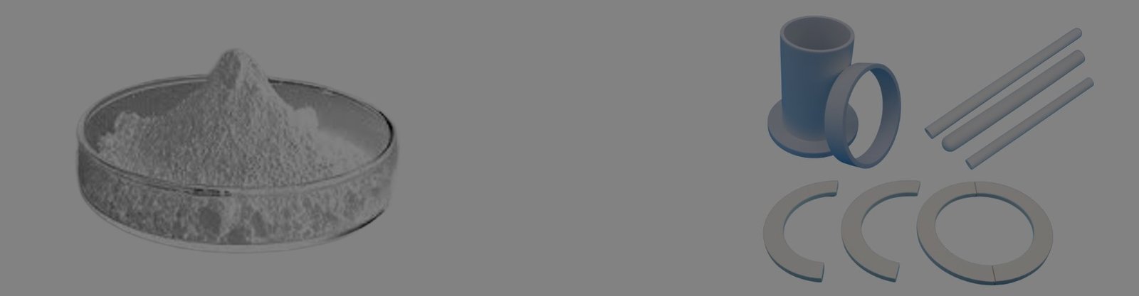
Boron Nitride Typical Material Grades & Forms
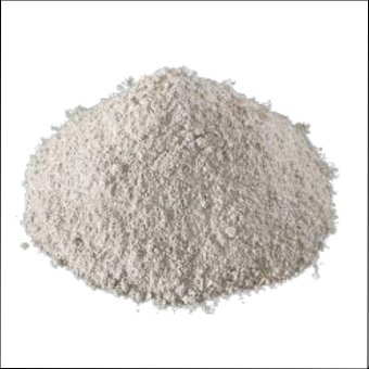
JingHui mainly supply hot-pressed hexagonal boron nitride ceramics, including:
-
High-purity h-BN ceramics
-
BN–SiO₂ composite ceramics
-
Machinable boron nitride ceramic grades
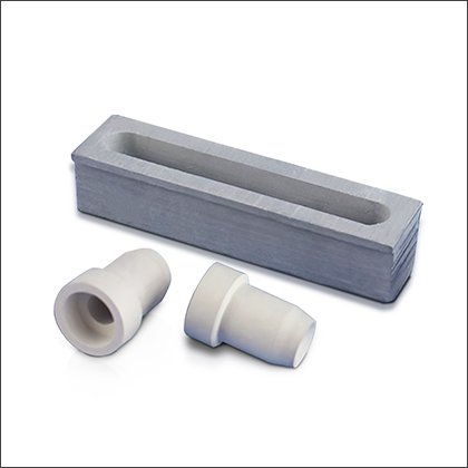
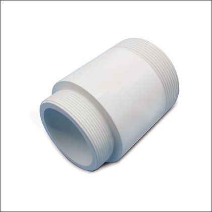
Common product forms include boron nitride plates, rods, blocks, sleeves, and custom-machined parts.
-
 Boron Nitride Sheet
 -
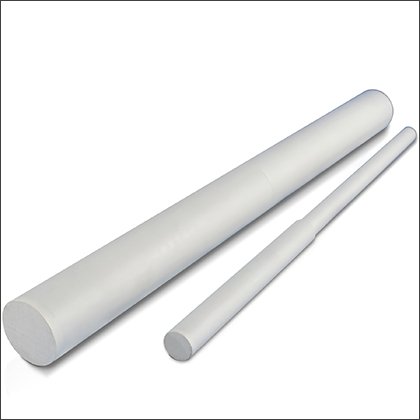 Boron Nitride Rod
 -
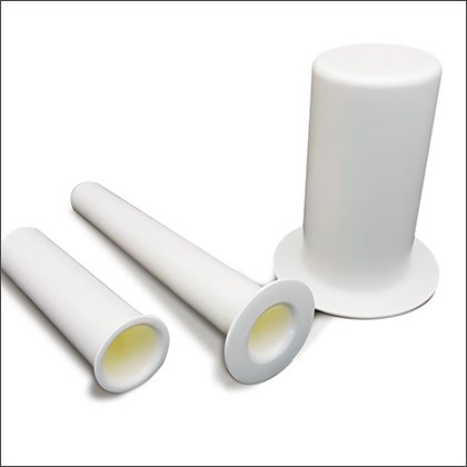 Boron Nitride Crucibles
 -
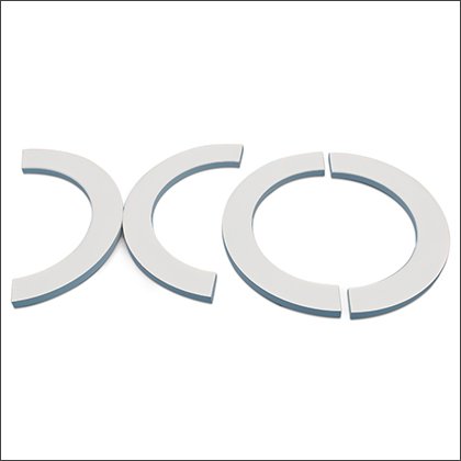
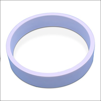 Boron Nitride Ring
 -
 Boron Nitride Nozzle
 -
 Boron Nitride Insulator
Key Features of Boron Nitride Ceramic

Boron nitride ceramic maintains structural integrity at temperatures up to 1800 °C in vacuum or inert atmospheres, outperforming alumina and graphite in non-oxidizing environments.

With high dielectric strength and low dielectric loss, h-BN ceramics are ideal for high-voltage, RF, and semiconductor applications.

The layered crystal structure provides intrinsic lubricity, reducing wear and eliminating the need for external lubricants.

Boron nitride ceramic does not react with molten aluminum, steel, or most non-ferrous metals, preventing contamination during casting or crystal growth.

Compared to most advanced ceramics, BN ceramics are easy to machine, allowing tight tolerances, thin walls, and complex geometries without edge chipping.
Typical Applications of Boron Nitride Ceramic
Semiconductor & Electronics
-
Wafer handling fixtures
-
Insulating components for ion implantation
-
Crucibles for silicon and GaN crystal growth
-
Heat spreaders for RF and power electronics
Vacuum & High-Temperature Furnaces
-
Electrical insulation parts
-
Support fixtures and setters
-
Thermal shields in inert gas environments
Molten Metal Processing
-
Aluminum and magnesium casting nozzles
-
Break rings and feed tubes
-
Non-wetting liners for molten metal contact
Aerospace & Advanced Energy
-
Radar-transparent components
-
High-temperature insulation parts
-
Sensor protection components
Related Materials
-
Alumina ceramics are advanced ceramics with excellent comprehensive properties, and they were researched early, are the most widely used, and are the most mature.
-
Zirconia ceramics are second only to alumina ceramics in terms of applicability and are very important advanced ceramics for structural applications.
-
Aluminum nitride ceramics are advanced ceramics with high thermal conductivity and insulation, and are often used in electronic packaging substrates and heat dissipation components.
-
Silicon nitride ceramics are high-strength, lightweight, and thermally shock resistant advanced ceramics commonly used in bearings and turbine components.
-
Silicon carbide ceramics are advanced ceramics with semiconductor properties and resistance to high-temperature corrosion, making them suitable for power devices and high-temperature structural components.
Manufacturing & Customization Capabilities
Boron nitride ceramic parts are produced through hot pressing to achieve high density and consistent properties.
We support:
-
Precision CNC machining and grinding
-
Complex geometries and thin-walled structures
-
Tight dimensional tolerances
-
Custom parts based on drawings or samples
Both prototype and small-to-medium batch production are available.
Boron Nitride vs Graphite vs Alumina
| Property | Boron Nitride (h-BN) | Graphite | Alumina |
|---|---|---|---|
| Electrical Insulation | Excellent | Conductive | Excellent |
| Self-Lubricating | Yes | Yes | No |
| Oxidation Resistance (Air) | ~900 °C | ~400 °C | >1500 °C |
| Machinability | Excellent | Excellent | Poor |
| Molten Aluminum Resistance | Excellent | Poor | Moderate |
Boron nitride ceramic is often selected when graphite is too reactive and alumina is too brittle or difficult to machine.
No. Hexagonal boron nitride ceramic is electrically insulating, unlike graphite, making it suitable for high-voltage and semiconductor applications.
Yes. Boron nitride ceramic performs exceptionally well in vacuum and inert atmospheres, with service temperatures up to 1800 °C.
Yes. Compared to most advanced ceramics, BN ceramics are relatively soft and machinable, allowing precise CNC machining without severe tool wear or chipping.
Yes. Custom boron nitride ceramic parts can be produced based on drawings or samples, including complex shapes, thin sections, and precision components.